Printed Circuit Boards (PCBs) are fundamental components in modern electronics, serving as the foundational platform that interconnects and supports electronic components. As technology evolves, understanding the diverse types of PCBs and their optimal applications becomes crucial for engineers, designers, and procurement specialists across industries. This comprehensive guide explores the classification of PCBs based on various parameters and provides detailed insights to help you select the right PCB type for your specific application needs.
Table of Contents
1. Classification by Structure and Layer Count
Single-Sided PCBs
Single-sided PCBs represent the simplest and most cost-effective PCB variant, featuring conductive copper traces on only one side of the insulating substrate . Components are mounted on one side, with their leads passing through holes to connect with the traces on the opposite side .
Key Characteristics:
– Simplified Design: Ideal for basic circuit implementations with minimal cross-over requirements
– Cost-Effective Manufacturing: Lower production costs due to reduced material requirements and simpler processes
– Space Considerations: Generally require more physical space for routing compared to multi-layer alternatives
Typical Applications:
– Basic consumer electronics including calculators and simple electronic toys
– Power supplies and relay circuits
– Radio and entertainment systems
– Industrial controls for simple functions
Double-Sided PCBs
Double-sided PCBs feature conductive layers on both sides of the substrate, connected through plated through-holes (PTHs) or vias that enable electrical continuity between layers . This configuration effectively doubles the available area for component placement and trace routing within the same board footprint.
Key Characteristics:
– Enhanced Circuit Density: Approximately twice the routing area of single-sided boards
– Versatile Interconnections: Multiple via technologies support diverse routing strategies
– Balanced Complexity: More complex manufacturing than single-sided but less than multi-layer boards
Typical Applications:
– Power conversion systems and UPS equipment
– Lighting control systems and LED drivers
– Automotive dashboards and control modules
– Test and measurement equipment

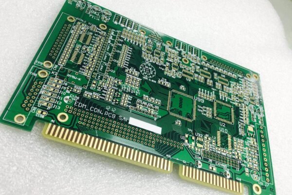
Multi-Layer PCBs
Multi-layer PCBs incorporate three or more conductive layers separated by insulating dielectric materials, laminated together under high pressure and temperature . These boards can range from 4 to over 50 layers, though practical commercial applications typically span 4-16 layers .
Key Characteristics:
– High Circuit Density: Multiple signal layers enable complex interconnections in compact form factors
– Improved Signal Integrity: Dedicated power and ground planes enhance noise immunity and EMC performance
– Enhanced Thermal Management: Distributed thermal paths improve heat dissipation
Typical Applications:
– Computer motherboards and server components
– Smartphones, tablets, and wearable devices
– Medical imaging and diagnostic equipment
– Aerospace and defense systems
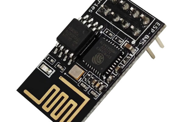
HDI (High-Density Interconnect) PCBs
HDI PCBs represent an advanced category of multi-layer boards incorporating higher wiring density per unit area through micro-vias, finer traces, and higher connection pad density . These boards enable more advanced component placement and significant size reduction.
Key Characteristics:
– Micro-Via Technology: Laser-drilled vias with diameters typically under 0.15mm
– Finer Feature Sizes: Trace width/spacing can reach 1mil/1mil (0.025mm) in advanced implementations
– Enhanced Signal Performance: Shorter signal paths improve high-frequency performance
Typical Applications:
– Smartphones and miniaturized consumer electronics
– High-performance computing and network processors
– Advanced medical implants and diagnostic equipment
– Military communications systems
2. Classification by Base Material and Flexibility
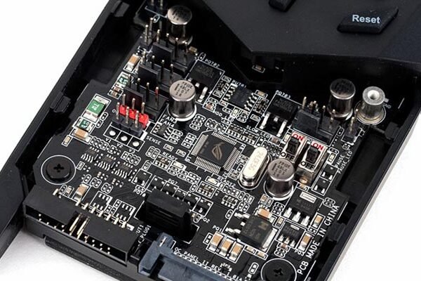
Rigid PCBs
Rigid PCBs utilize solid, inflexible substrate materials that provide structural stability and component support . The most common base material is FR-4, a glass fiber-reinforced epoxy laminate valued for its mechanical strength, thermal stability, and electrical insulation properties .
Key Characteristics:
– Dimensional Stability: Maintains shape under mechanical stress and thermal cycling
– Component Support: Provides secure mounting platform for heavy components
– Manufacturing Simplicity: Well-established processes with high predictability
Typical Applications:
– Computer peripherals and motherboards
– Industrial control systems
– Power supplies and conversion equipment
– Automotive entertainment and control units

Flexible PCBs
Flexible PCBs (FPCs) utilize pliable base materials such as polyimide (PI) or polyester (PET) that can bend, fold, or twist during operation . These boards typically use rolled annealed copper foil to enhance fatigue resistance.
Key Characteristics:
– 3D Assembly Capability: Can conform to available spaces in complex mechanical assemblies
– Dynamic Flex Capability: Withstands repeated bending cycles (10,000-100,000+ depending on materials)
– Weight Reduction: Significantly lighter than equivalent rigid boards (60-80% weight reduction)
Typical Applications:
– Mobile phone displays and connections
– Wearable technology and medical sensors
– Automotive lighting systems and seat sensors
– Industrial robotics with moving components

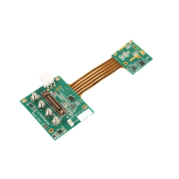
Rigid-Flex PCBs
Rigid-flex PCBs hybridize rigid and flexible technologies by integrating rigid board sections with flexible interconnections in a single, continuous structure . This approach eliminates discrete connectors between board segments, enhancing reliability while maintaining the benefits of both technologies.
Key Characteristics:
– Reduced Interconnection Points: Fewer connectors improve reliability and reduce failure points
– 3D Packaging Efficiency: Optimizes use of available volume in complex enclosures
– Improved Signal Integrity: Continuous impedance control across board sections
Typical Applications:
– Aerospace and satellite systems
– Military communications equipment
– High-reliability medical devices
– Advanced automotive control systems
3. Classification by Specialized Materials and Applications
High-Frequency PCBs
High-frequency PCBs are engineered to operate at radio frequencies (>10GHz) with minimal signal loss and consistent impedance characteristics . These boards utilize specialized dielectric materials with controlled dielectric constant (Dk) and dissipation factor (Df) such as PTFE, RO4000® series, and ceramic-filled laminates.
Key Characteristics:
– Controlled Dielectric Properties: Stable Dk values across frequency and temperature variations
– Low Loss Tangent: Minimizes signal attenuation at high frequencies
– Precise Impedance Control: Tight tolerance impedance lines (typically 50Ω±2%)
Typical Applications:
– 5G infrastructure and millimeter-wave equipment
– Radar and satellite communication systems
– RF identification (RFID) readers
– High-speed wireless backhaul equipment
Metal-Core PCBs (MCPCBs)
Metal-core PCBs incorporate a metallic base layer (typically aluminum or copper) to provide superior thermal management for high-power applications . The metal core acts as a heat spreader, transferring thermal energy away from critical components.
Key Characteristics:
– Enhanced Thermal Conductivity: Aluminum cores provide 1-2W/m·K, copper up to 400W/m·K
– Improved Power Density: Enables higher power operation in confined spaces
– Mechanical Robustness: Metal substrate provides structural integrity
Typical Applications:
– High-power LED lighting systems
– Power converters and motor drives
– Automotive power electronics
– Photovoltaic system controllers
High-Speed Digital PCBs
High-speed digital PCBs are optimized for signal integrity in applications with data rates exceeding 5Gbps . These boards employ carefully controlled dielectric materials, precise impedance matching, and advanced layout techniques to maintain signal quality.
Key Characteristics:
– Low-Loss Materials: Specialty laminates with Df<0.005 at high frequencies
– Advanced Layout Techniques: Matched length routing, minimized via stubs, and optimized return paths
– Comprehensive SI/PI Analysis: Extensive simulation to ensure signal and power integrity
Typical Applications:
– Network switches and routers
– Data center computing hardware
– High-definition video processing
– Artificial intelligence accelerators
4. Application-Specific PCB Selection Guide
Table: PCB Selection Guide by Industry and Application
| Industry | Recommended PCB Types | Key Considerations | Typical Layer Count |
| Consumer Electronics | HDI, Flexible, Rigid-Flex | Miniaturization, cost sensitivity, high volume | 4-10 layers (HDI), 1-2 layers (flex) |
| Automotive | Metal-core, Rigid, Flexible | Thermal management, vibration resistance, long-term reliability | 2-8 layers (rigid), 1-4 layers (flex) |
| Aerospace/Defense | High-frequency, Rigid-Flex, Multilayer | Extreme environments, signal integrity, maximum reliability | 8-20+ layers |
| Medical Devices | Flexible, HDI, Ceramic-based | Miniaturization, reliability, biocompatibility (implants) | 4-12 layers (HDI), 1-4 layers (flex) |
| Industrial Equipment | Thick-copper, Metal-core, Multilayer | Power handling, thermal performance, noise immunity | 2-10 layers |
| Telecommunications | High-frequency, High-speed Digital | Signal integrity at high frequencies, impedance control | 8-24 layers |
5. PCB Material Composition and Structure
Understanding PCB construction begins with recognizing its fundamental layers and materials:
Basic PCB Layer Structure
•Base Material (Substrate): Typically FR-4 glass epoxy, polyimide (flexible boards), or specialized high-frequency materials
•Copper Layer: Electrodeposited or rolled copper foil, typically 0.5-6.0 oz/ft² thickness
•Solder Mask: Polymer layer applied over copper traces for insulation and protection, typically green or other colors
•Silkscreen: Identification layer with component designators, logos, and other markings

Advanced Material Options
•Ceramic Substrates: Aluminum oxide (Al₂O₃) or aluminum nitride (AlN) for exceptional thermal performance
•Low-Loss Thermoplastics: Liquid Crystal Polymer (LCP) for millimeter-wave applications
•Composite Materials: Mixed dielectric constant materials for optimized performance/cost balance
6. Future Trends in PCB Technology
The PCB industry continues to evolve, driven by emerging technologies and application demands:
•Miniaturization Continuation: Further reduction in feature sizes with increased adoption of mSAP (modified Semi-Additive Process) manufacturing
•Embedded Components: Resistors, capacitors, and semiconductors integrated within the PCB structure
•Sustainable Materials: Development of halogen-free, biodegradable, and recyclable base materials
•Advanced Thermal Management: Integration of novel cooling technologies including vapor chambers and thermal vias
•Additive Manufacturing: Increasing adoption of inkjet and aerosol printing for prototyping and specialized production
Conclusion: Selecting the Optimal PCB Solution
Choosing the right PCB type involves careful consideration of electrical, mechanical, thermal, and economic factors aligned with your specific application requirements. As this guide demonstrates, the PCB landscape offers diverse solutions ranging from simple single-sided boards to sophisticated HDI and rigid-flex configurations.
For optimal results:
– Prioritize Requirements: Clearly define performance, reliability, and cost targets before selection
– Engage Early Collaboration: Involve PCB manufacturers during the design phase to leverage their expertise
– Consider Total Cost: Evaluate not just board cost but assembly, testing, and potential field failures
– Plan for Evolution: Select technologies that accommodate potential future feature additions or performance enhancements
The continuing innovation in PCB technologies ensures that electronic designers have increasingly sophisticated tools to solve complex interconnection challenges across all industries. By understanding the capabilities and optimal applications of each PCB type, engineers can make informed decisions that balance performance, reliability, and cost-effectiveness for their specific applications.