

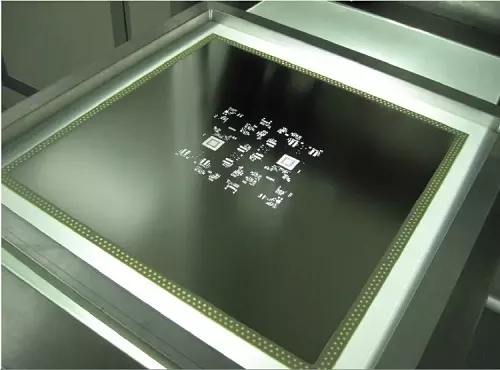
Stencil
The design of stencil opening is one of the main means to optimize the SMT process, and it is also an important factor affecting the quality of the SMT process. The opening design of the stencil mainly includes the shape of the hole, the size of the hole, and the stencil thicknesses.
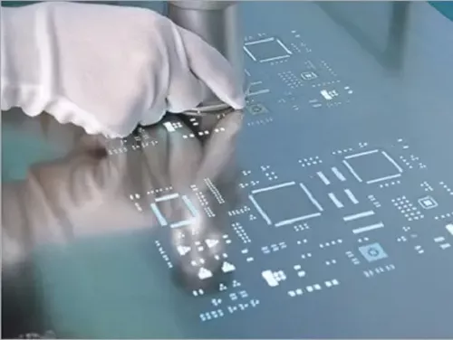
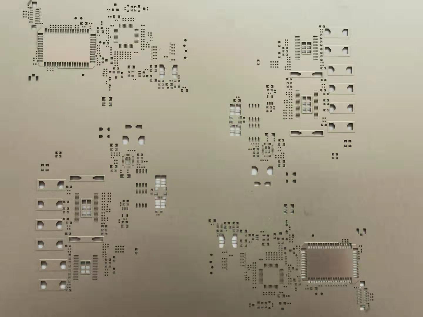
The SMT stencil is designed for printing solder paste onto the circuit board. Therefore, the stencil surface will be engraved with many openings. When printing the solder paste, the solder paste should be applied on the stencil. The board will be placed under the stencil, and then a scraper (usually a scraper, because the solder paste is similar to a toothpaste-like viscous material) is brushed over the stencil surface with the solder paste, and the solder paste is squeezed. It will flow down from the opening of the stencil and stick it to the top of PCB board. When the stencil is removed, it will be found that the solder paste has been printed on the board.
To put it simply, the stencil is like a hood to be prepared when painting, and the solder paste is equivalent to lacquer. The hood is engraved with the pattern you want. When you spray the lacquer on the hood, the desired pattern appears.
SYS Technology Co., Ltd. specializes in various SMT stencil fabrication, solder paste, red glue research and development, cutting magnetic steel sheets, patch fixtures, furnace fixtures, machining, production and SMT accessories industry for many years. Over the years of continuous accumulation, the customer base has accumulated as many as thousands, covering the Pearl River Delta, the Yangtze River Delta, Northeast China, North China and other regions.
SysPCB – Professional Stencil Production
With superb technology, high-quality service and advanced management model, we have won wide recognition in the industry, and are a fast-growing and reputable SMT formwork manufacturer in the formwork industry in recent years, with a well-trained sales force With experienced technical engineers, we have accumulated rich practical experience in stencil opening design, printing effect, and material selection, and are ahead of the same industry in major aspects such as tin release performance and tin bead protection in printing, so as to provide customers with excellent service.
It solves the bad phenomena such as virtual soldering, continuous soldering and solder balls in the SMT placement process, and ensures that customers successfully take the key step from solder paste to reflow soldering process in the production process. It has achieved the effect of no-cleaning; it has brought effective cost control to various enterprises and institutions, and greatly improved the efficiency of electronic industrial production and product quality.
Since its establishment, the company has always attached importance to the training of company personnel and the introduction of advanced equipment. With high-quality talents as the core, high-precision equipment as the foundation, and advanced technology as the foundation, the company provides customers with more thoughtful and faster services.
About laser stencil cutting:
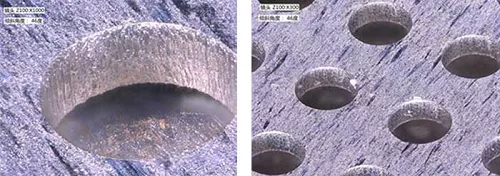
1、 High precision laser cutting technology
The laser template cutting accuracy can reach 3 μ m, and the hole position and shape accuracy reach the top level in the industry.
1. The equipment adopts high-end optimized fiber laser source and professional optical path design, with a smooth and burr free cutting surface. Combined with post-treatment processes such as characteristic polishing, it significantly improves the demolding performance of the steel mesh;
2. The opening is designed with an inverted cone shape to optimize the efficiency of solder paste release, ensuring clean and fast printing, and accurately covering the solder pads to the desired shape and position.
2、 Intelligent data-driven processing system
3. Based on genuine professional software for data processing, it supports arbitrary scaling of opening size/shape, and can fully customize and adjust opening parameters according to customer needs;
6. Equipped with repositioning function to achieve precise hole filling, with a minimum opening of up to 30 μ m, avoiding the risk of thermal deformation and ensuring ultra precision steel mesh forming;
7. A professional team combines customer needs and industry experience to optimize design through simulation, ensuring the performance and long-term reliability of steel mesh printing and welding.
3、 Multi scenario applicability extension
4. Support full-size steel plate cutting to meet diverse printing needs;
5. The cutting thickness covers 0.03mm-0.40mm, compatible with thin/thick material processing, and can be extended to precision metal sheet and component manufacturing.
4、 Whole process quality assurance system
8. Half cut optical recognition points have high contrast and clear black and white boundaries; Cooperate with strict quality inspection procedures to ensure accurate steel mesh size, smooth appearance, and long service life;
9. Adopting imported steel plates from Japan and domestically produced high-end AB plastic sealed mesh frames, the steel mesh tension stability reaches the industry benchmark, is resistant to solvent cleaning, and can be used for a long time without breaking the mesh.
Structured highlights
1. Clear technical layering: unfolding step by step from core processes to scenario applications
2. Data quantification presentation: Key indicators such as 3 μ m accuracy and 30 μ m opening enhance persuasiveness
3. Quality closed-loop design: covering the entire process of material selection, processing technology, and testing standards
4. User value orientation: highlighting customization capabilities and long-term reliability advantages
3 types of SMT stencil production process
According to the processing methods, basically the classification of SMT stencil can be divided into three categories, that is: chemical etching process, laser cutting process, electroforming process.
These are the differences in production methods, but the preliminary steps are basically the same. For example, customers provide ready-made PCB circuit boards, which are scanned and drawn into production files; or they are directly provided with drawings (i.e. PCB design files or Gerber files etc. that can be processed by computers), these are sent to the SMT stencil manufacturer, and then the engineering department of the SMT stencil manufacturer conducts pre-production design processing to make finished documents suitable for final processing, and then get it to the production department for production.
solder paste printing principle
With the development of SMT stencil, more than 95% of the stencil in the SMT processing industry is made by laser cutting. Next, let’s briefly introduce the three production methods, advantages and disadvantages of corresponding SMT stencil:
1. Chemical etching: Apply a layer of acid-proof glue on the steel plate, remove the glue where the opening is needed, exposing the steel plate, and corrode the steel plate with acid to form an opening. The effect of using this kind of stencil is not very good.
2. Laser cutting: It is very simple to use laser to directly drill holes in the place where the opening is needed. This kind of steel plate is the most used and the price is relatively cheap.

3. Electroforming: This kind of stencil is based on laser cutting. Then inner wall and the opening chamfer are electroformed at the opening, so that the inner wall of the opening is very smooth, which is good for solder paste printing. This kind of steel plate is very expensive and is not used much, unless there are special requirements for the SMT process, it is generally not used.
If you need SMT stencil, it is best to purchase SMT stencil according to your actual situation. If the opening is very simple, you do not need to mount very precise components (including 0.5mm or below pitch IC, 0201 chip material, etc.), chemical etching method can fully meet your needs.
So what are the advantages and disadvantages of laser stencil compared with other type stencils?
(1) Advantages:
Compared with etched stencil and electroformed stencil. Laser SMT stencil is simple to make, fast, accurate, easy to use, and affordable. After the laser stencil is electropolished, the quality is better and the effect is better. At present, most stencil of SMT processing on the market use laser cutting.
(2) Disadvantages:
The thickness is fixed one, the ladder stencil cannot be made, and the treatment of irregular shapes of rounded corners and chamfers is not perfect.