

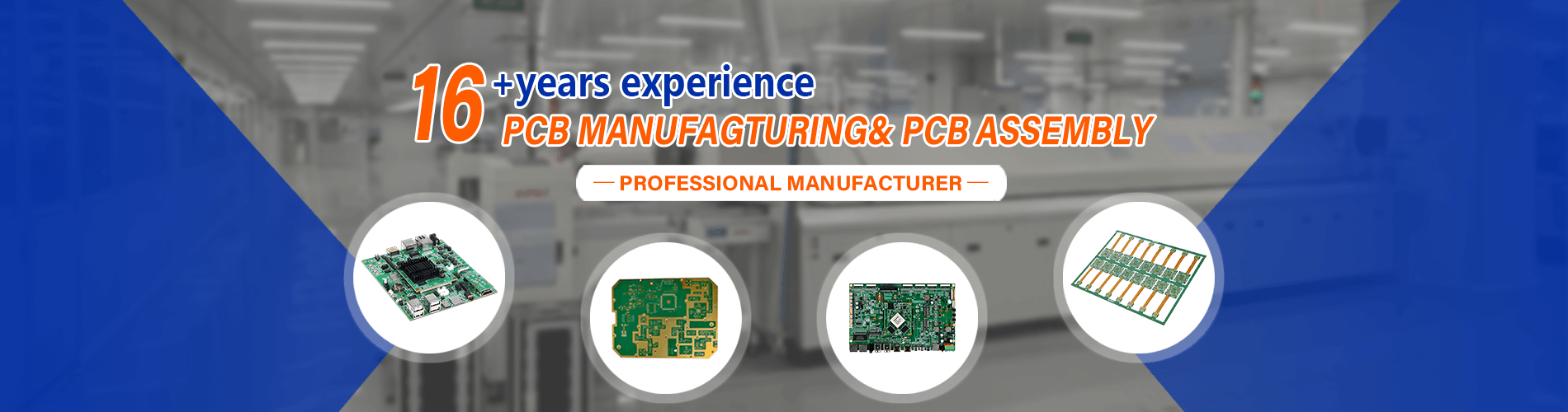

PCB Assembly
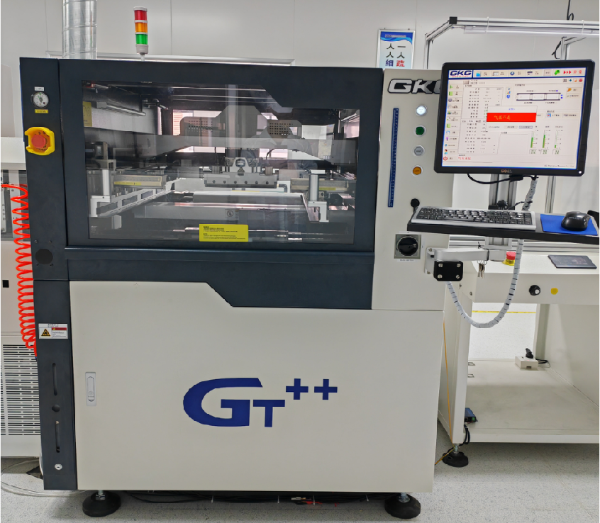
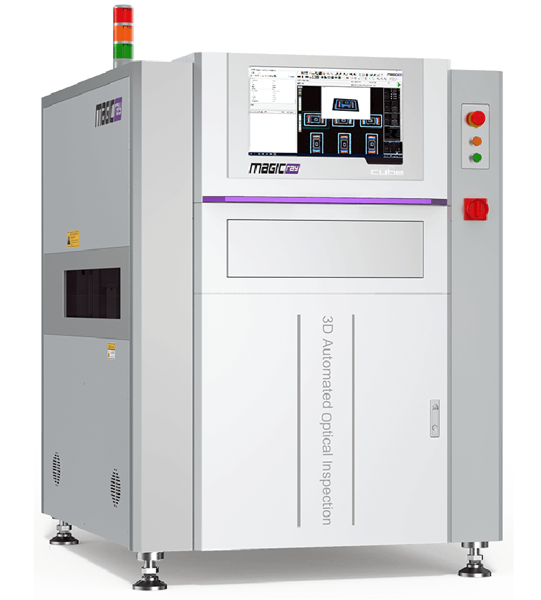
SysPCB provides PCBA assembly, from prototype to production volume. Our professional SMT factory has advanced equipment, such as the world-class stencil printing, SMT chip pick & place, solder reflow, and in-line testing and steel manufacturing. AOI test machine and X-ray testing machines for quality check.
SysPCB offers turn-key PCB assembly services in prototype quantities or low-volume to mid-volume production runs. We handle the whole process including: ordering all the components, PCB manufacturing, PCB assembly, testing and final shipment. We are capable of assembling BGA, Micro-BGA, QFN and other leadless package parts.
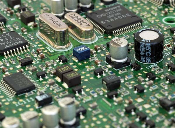
Surface Mount Technology
All products of SysPCB follow IPC class II standards. With 16 years experience of mounting BGA, UBGA, CSP and small profile passive componentss down to 0201, SysPCB offers a cost effective high yield solution to any SMT requirement.
Through Hole
Capabilities to place tape and reeled radial components. Maximum PCB size is 40″ x 40″. Placement rates reach 15000 pieces per hour with an accuracy of 99% minimizing component loss.
RoHS Regulations
All SysPCB’s production are RoHS compliant, we only use lead free material.
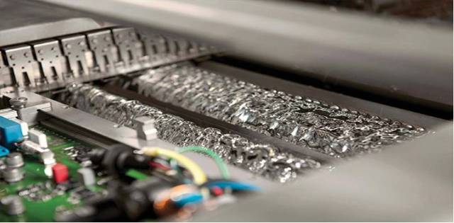
Selective Wave Solder
With the Selective Wave soldering machines, SysPCB achieves consistent quality and process control when assembling boards with multiple ground and power planes, high-current connectors or A-typical distribution of components. All AOI tested before shipping.
Conformal coating
Both dip-coating and vertical spray coating is available. Protective non conductive dielectric layer that is applied onto the printed circuit board assembly to protect the electronics from damage due to contamination, salt spray, moisture, fungus, dust and corrosion caused by harsh or extreme environments. When coated, it is clearly visible using a clear and shiny material.
【PCB Assembly Product Description】
1. Circuit board PCBA overall solution
2. PCB assembly, PCB/PCBA design, PCBA copy board
3. Customized processing PCBA/OEM/EMS (electronic manufacturing service)
4. SMT&DIP&PTH&BGA assembly
5. Provide component procurement services
6. Fast PCBA prototype
7. X-ray test, internal circuit test (ICT), functional test (FCT)
8. Small and medium batches fast turnaround
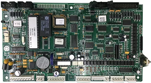
PCBA Manufacturing Services/PCB Assembly
- Customers provide: PCB files, PCB fabrication requirements, bill of materials, assembly or soldering technical requirements.
- One-stop PCBA service: production of 1-32 layers PCB, assembly parts/material procurement, SMT production, PCBA testing, PCBA packaging, PCBA delivery.
PCBA Manufacturing Quality
| Authentication information | UL, SGS, TUV, BV, ROHS, ISO9001:2015, TS16949 |
| PCBA production equipment | – Jikangda solder paste printing machine – Panasonic MVⅡ-F – Panasonic JUKI-2050M placement machine -GKG Automatic solder paste printing machine – Reflow oven – Wave soldering machine |
| PCBA testing equipment | – ORT machine – Constant temperature – Humidity test chamber – 3D coordinate measuring instrument – ROHS testing machine – X-ray |
| PCBA testing capabilities | – ICT (internal circuit testing) – FCT (functional circuit testing) – BGA X-ray testing |
| Range of processable components | – 0201, 0402, 0603, 0805, 1206, 1608, 2125, 3216 – Micro QFP 0.3mm – Flip Chip, BGA, Connector – BGA 0.3mm |
| Materials | FR-4/FPC/aluminum base/high TG/halogen-free/high frequency/CEM-1/CEM-3/FR-1 |
| CCL | Kingboard Shengyi Nanya Grade A material |
PCBA production(PCB Assembly) lead time
After the OEM contract is signed and the engineering documents are confirmed, the sample delivery time is usually 7-10 working days.
For mass production, according to customer demand, it can be delivered in batches, one part at a time.
PCBA Manufacturing Supplementary Information
1. After the sample is confirmed to be OK, start mass production.
2. The plug-in components can only be positioned once, and the minimum distance between the components and the PCB will remain unchanged.
3. The positioning holes and grounding holes will be protected with high temperature resistant tape.
4. EPE anti-static packaging is used to prevent shocks and other problems.
PCBA Shipping
Standard packaging
Each PCBA board is placed in an anti-static bag, then covered with a bubble bag, and finally placed in a specially processed carton.
PCB assembly process overview
The PCB assembly process is an essential element of the electronics production lifecycle. PCB manufacturing and assembly employs many new areas of technology. The various stages in the PCB assembly process including adding solder paste to the board, pick and place of the components, soldering, inspection and test. All these processes are required, and need to be monitored to ensure that product of the highest quality is produced. The PCB assembly process described below assumes that surface mount components are being used as virtually all PCB assembly these days uses surface mount technology.
1. Solder paste
Prior to the addition of the components to a board, solder paste needs to be added to those areas of the board where solder is required. Typically these areas are the component pads. This is achieved using a solder screen.
The solder paste is a paste of small grains of solder mixed with flux. This can be deposited into place in a process that is very similar to some printing processes.
Using the solder screen, placed directly onto the board and registered in the correct position , a runner is moved across the screen squeezing a small mount of solder paste through the holes in the screen and onto the board. As the solder screen has been generated from the printed circuit board files, it has holes on the positions of the solder pads, and in this way solder is deposited only on the solder pads.
The amount of solder that is deposited must be controlled to ensure the resulting joints have the right amount of solder.
2. Pick and place
During this part of the assembly process, the board with the added solder paste is then passed into the pick and place process. Here a machine loaded with reels of components picks the components from the reels or other dispensers and places them onto the correct position on the board.
The components placed onto the board are held in place by the tension of the solder paste. This is sufficient to keep them in place provided that the board is not jolted.
In some assembly processes, the pick and place machines add small dots of glue to secure the components to the board. However this is normally done only if the board is to be wave soldered. The disadvantage of the process is that any repair is made far more difficult by the presence of the glue, although some glues are designed to degrade during the soldering process.
The position and component information required to programme the pick and place machine is derived from the printed circuit board design information. This enables the pick and place programming to be considerably simplified.

3. Soldering
In order to enable the components added to the board, either leaded or SMT to solder to the board easily, exposed areas of the board are normally “tinned” or plated with solder. Occasionally boards, or areas of boards may be gold plated. This may be applicable if some copper fingers are to be used for edge connections. As the gold will not tarnish, and it offers good conductivity it provides a good connection at a low cost.
Once the components have been added to the board, the next stage of the assembly, production process is to pass it through the soldering machine. Although some boards may be passed through a wave soldering machine, this process is not widely used for surface mount components these days. If wave soldering is used, then solder paste is not added to the board as the solder is provided by the wave soldering machine. Rather than using wave soldering, reflow soldering techniques are used more widely.
4. Inspection
After the boards have been passed through the soldering process they are often inspected. Manual inspection is not an option for surface mount boards employing a hundred or more components. Instead automatic optical inspection is a far more viable solution. Machines are available that are able to inspect boards and detect poor joints, misplaced components, and under some instances the wrong component.
5. Test
It is necessary to test electronic products before they leave the factory. There are several ways in which they may be tested. Further views of test strategies and methods may be found on the “Test and Measurement” section of this website.
6. Feedback
To ensure that the manufacturing process is running satisfactorily, it is necessary to monitor the outputs. This is achieved by investigating any failures that are detected. The ideal place is at the optical inspection stage as this generally occurs immediately after the soldering stage. This means that process defects can be detected quickly and rectified before too many boards are built with the same problem.
Summary
PCB Assembly consists of several digital elements that allow the performing of an device. PCB Assembly services involve multi-stage procedures that include putting elements on a PCB board, soldering them in place, and checking and examining these elements. As part of any development process it is normally advisable to make a prototype before committing to full production. The same is true of PCB Assembly where a prototype is normally manufactured and tested before full production.
Application Areas
PCBA is widely used in various electronic products, including:
- Television: Core components for electrical connections and signal transmission.
- Computers: Key components like motherboards and expansion cards.
- Mobile Phones: Internal circuit board assemblies.
- Automotive Electronics: In-vehicle control systems, sensors, etc.
- Medical Equipment: Circuit board assemblies inside precision instruments.
Procedure of PCBA maintenance(PCB Assembly)
In the PCBA production process, due to the improper operation of the production personnel or the quality of the materials, there are often defective PCBA boards. At this time, the defective PCBA boards need to be repaired. There are generally PCBA maintenance engineers in the PCBA factory. When repairing the board, it is necessary to follow a certain maintenance process.
The process of PCBA maintenance is as follows:
Visual inspection of PCBA → measure all POWER → poor power-on test → repair according to the defective phenomenon → self-inspection after repair → test fixture test → full visual inspection
The tools that need to be prepared for PCBA maintenance are: oscilloscope, digital meter, constant temperature soldering iron, heat gun, needle nose pliers, diagonal pliers, tweezers.
1. Visual inspection of PCBA
Mainly check whether the PCBA has obvious appearance defects. Such as: short circuit, missing parts, orientation reversed components, wrong components, etc.
2. Measure all POWER
Mainly measure whether the power supply is short-circuited to ground.
3. Poor power-on test
Use the test fixture DOUBLE CHECK after power-on.
4. Repair according to the defective phenomenon
Repair according to the defective phenomenon and the circuit principle. You can refer to the maintenance instructions provided by production engineer.
5. Self-check after maintenance
After maintenance, the maintenance part needs to be self-checked. Main inspection: short circuit, empty solder, solder ball, solder dross and appearance of solder joint
6. Test fixture test
Use a test fixture to check whether the PCBA is repaired OK.
7. Full visual inspection
Full inspection of repaired products. By repairing the defective PCBA board, the scrap of the board can be reduced and the production cost of the factory can be reduced.

Cooperation process of PCBA contract manufacturing
At present, more and more PCBA manufacturers provide labor and material contracting services, which can free customers from the manufacturing process and save investment costs in electronic material procurement, warehousing, outsourcing, logistics and personnel.
The cooperation mode of PCBA contract manufacturing can effectively save customers’ time, labor, storage and other costs, and only need to provide production data and necessary process confirmation during the production process. Although the price may be a little more expensive than producing it yourself, the overall cost is lower. Customers only need to provide product information, such as: PCB files, BOM forms, coordinate files, installation files, etc., other production and processing can be handed over to the factory. So, what is the cooperation process of PCBA contract manufacturing? Today, China PCBA contract manufacturer will take you to learn more about it.
1. The manufacturability evaluation of PCBA, and the information provided by the customer for the factory quotation.
2. After business communication, both parties confirm cooperation and sign a contract.
3. After the customer completes the product design, the engineering documents such as Gerber file and BOM list are handed over to the manufacturer. The manufacturer will have specialized process personnel to review, confirm, and evaluate key points such as stencil printing, SMT technology, and plug-in technology.
4. After the material procurement, inspection, and material preparation are completed, the production will be scheduled according to the PMC plan.
5. SMD chip mounting, online production and processing of materials, quality inspection after reflow soldering, AOI inspection, DIP plug-in, wave soldering and other processes.
6. Quality inspection by the quality department. The quality department conducts random inspections on some products or full inspections, and repairs defective products after they are found.
7. Packaging and transportation and after-sales service. Packaging and transportation should be carried out after all product processed quality inspections. The packaging material adopts anti-static packaging bags. If the customer has special requirements, the packaging will be carried out according to the customer’s needs, and the after-sales service will be provided.
About SysPCB
We are a reliable Chinese PCB manufacturer, dedicated to becoming a long-term partner for our customers. We provide reliable PCB production services to ensure a high level of cooperation with customers in terms of quality, delivery time, and after-sales support.