One-Stop Turnkey China PCB Manufacturer
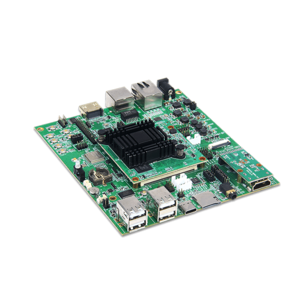
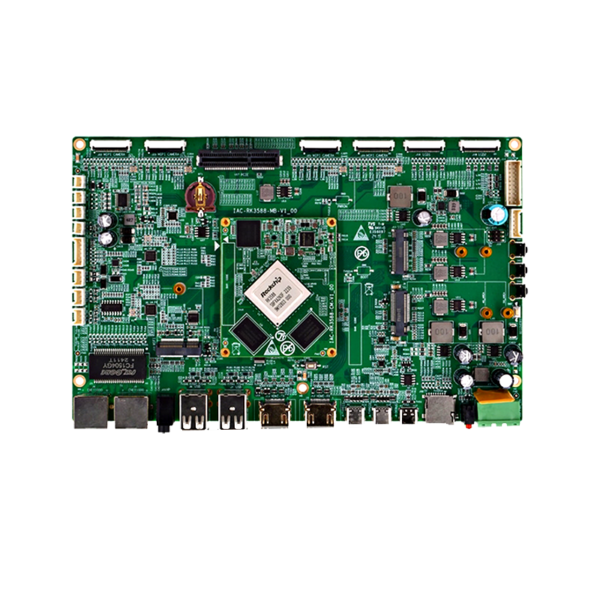
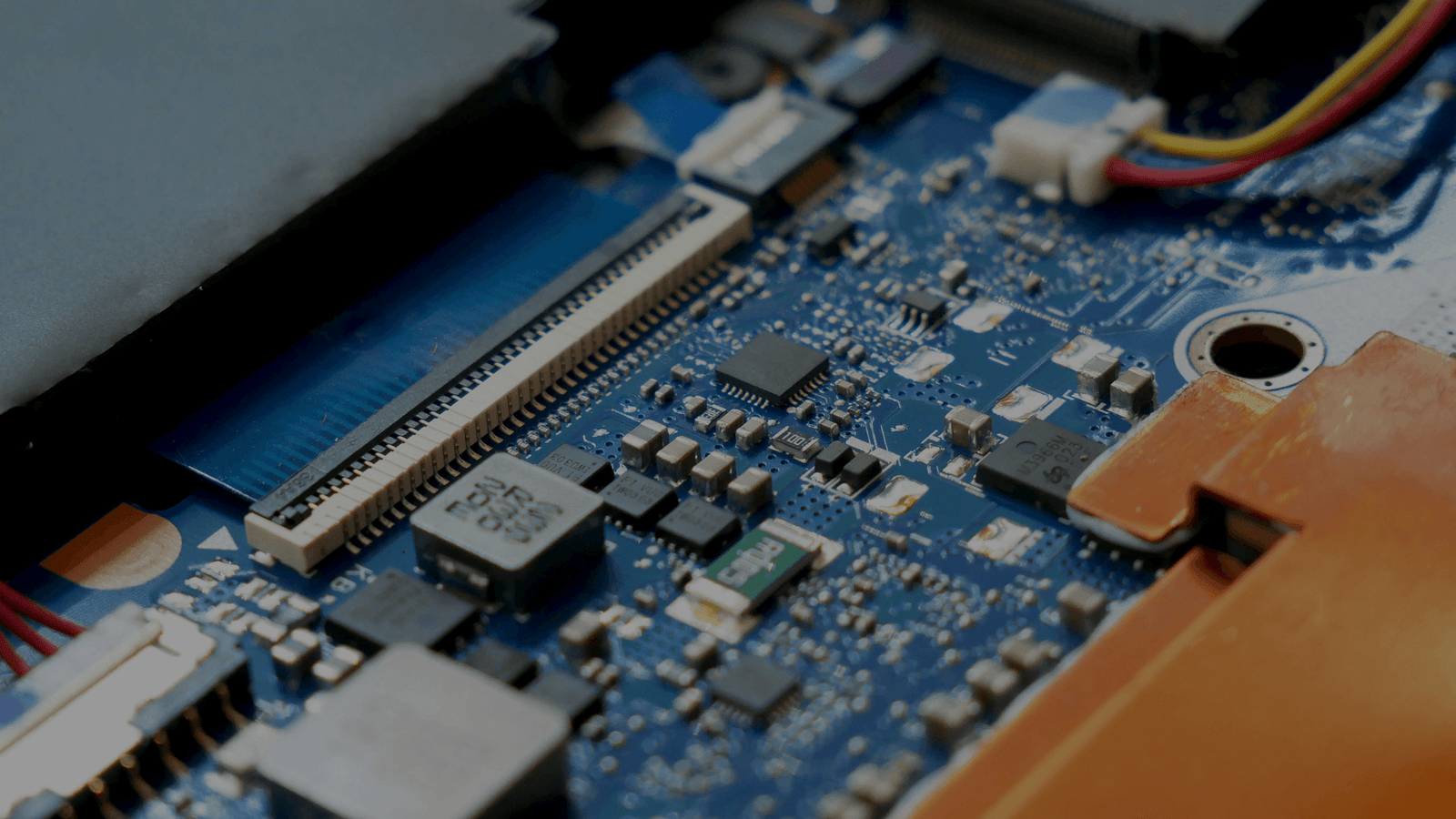
MorePCB support full Turn-Key PCB Assembly includes PCB fabrication, parts sourcing,
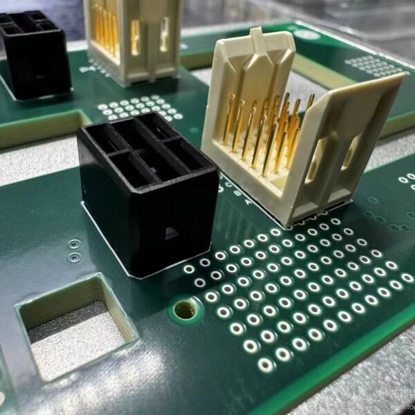
PCB assembly, QC inspection, and functional test.

 English
MorePCB support full Turn-Key PCB Assembly includes PCB fabrication, parts sourcing,
PCB assembly, QC inspection, and functional test.
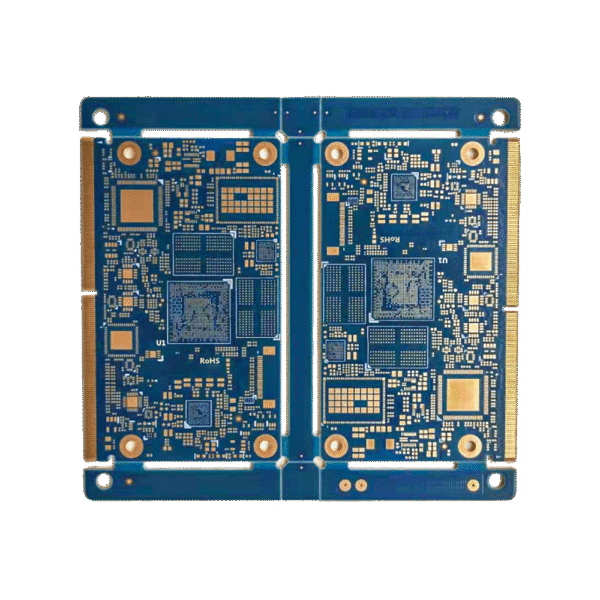
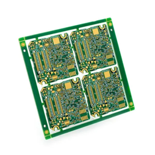
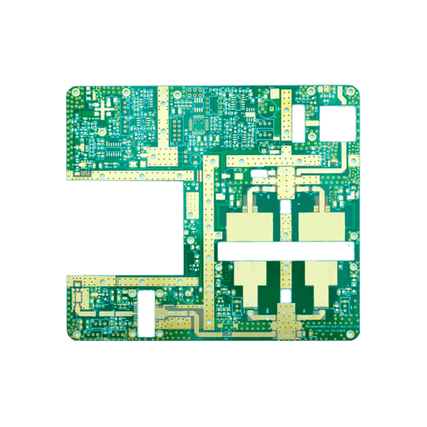
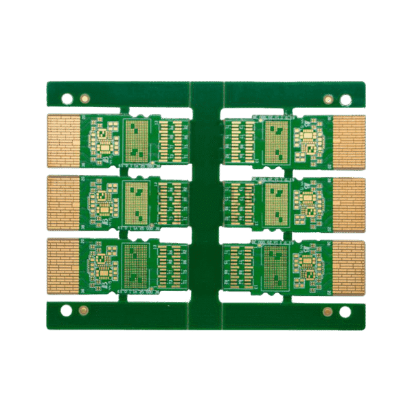
SYS PCB, as a leading PCB manufacturer in China, has been providing support to global customers for over 15 years. Its products are widely used in high-tech industries such as industrial control, automotive, security, medical, and communication.
Learn More
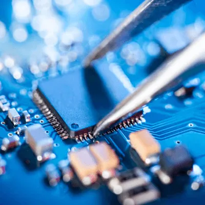
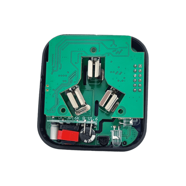
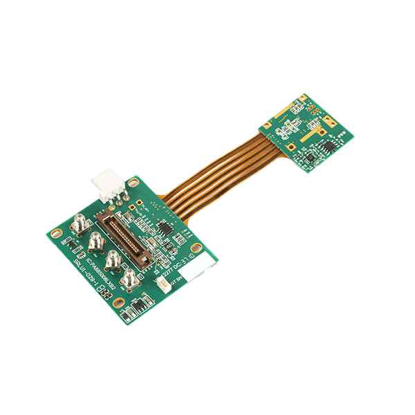
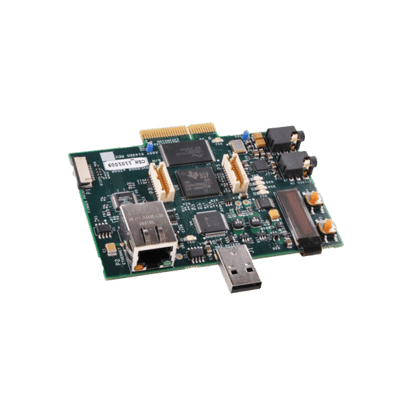
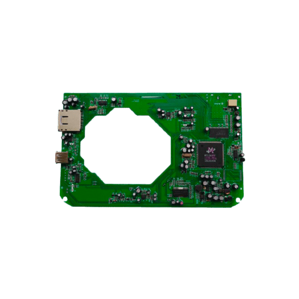
SysPCB is a leading PCB manufacturer in China. We offer better one-stop PCB assembly services at a lower price, from PCB manufacturing, SMT assembly to final PCB testing. We always focus on fast PCB prototype design and one-stop PCB assembly services, and are a leading China PCB assembly manufacturer in the industry
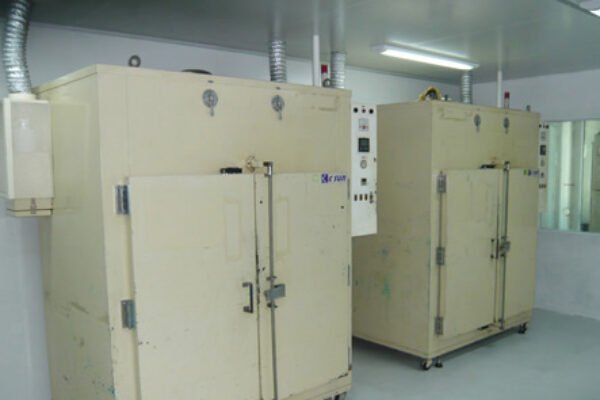
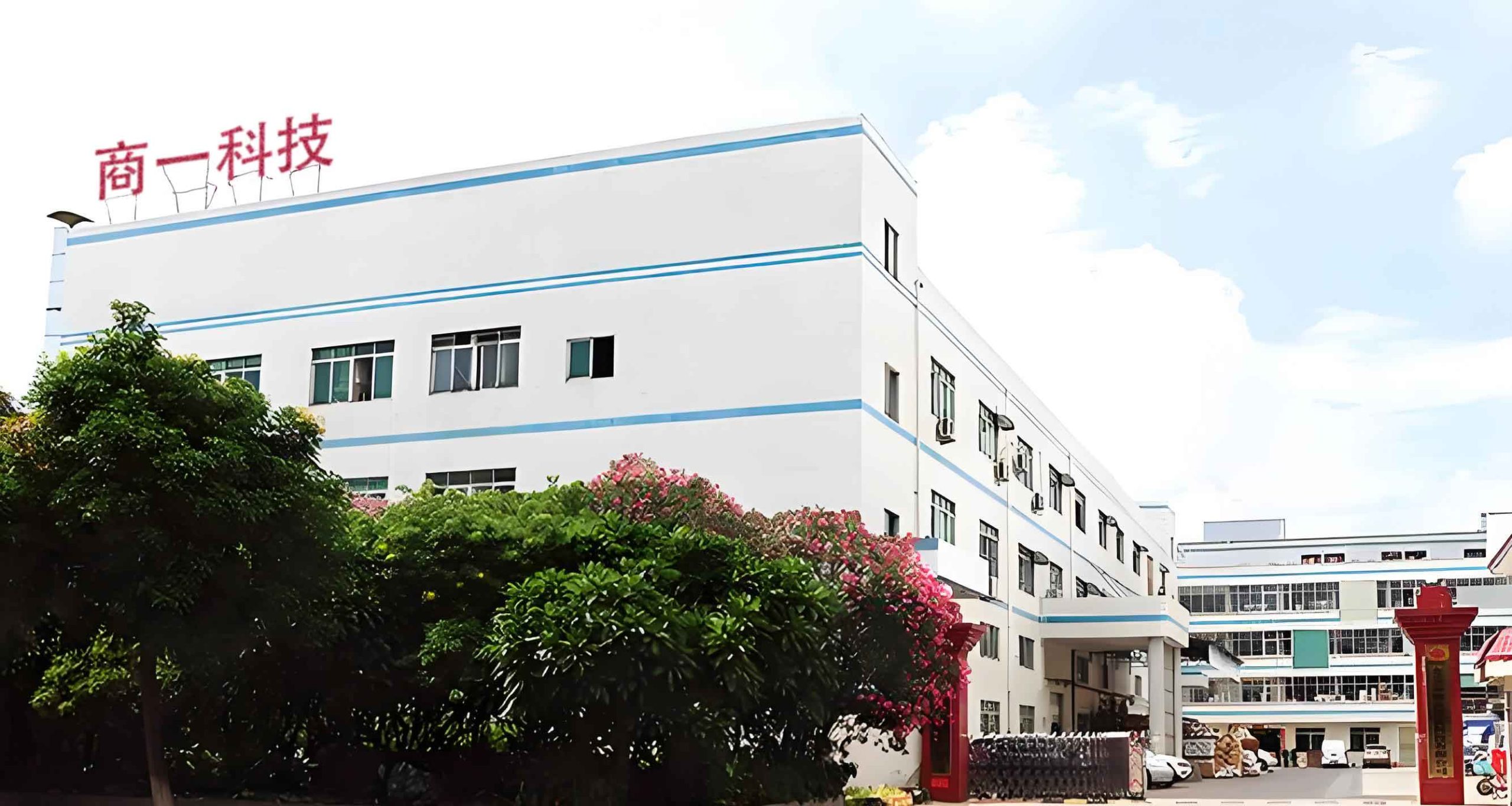
Sys Technology Co., Ltd. is a professional PCB manufacturer in China. We have been manufacturing PCBs in China since 2008. We have two Chinese PCB factories with 160 PCB professionals and 30 employees in the SMT factory.
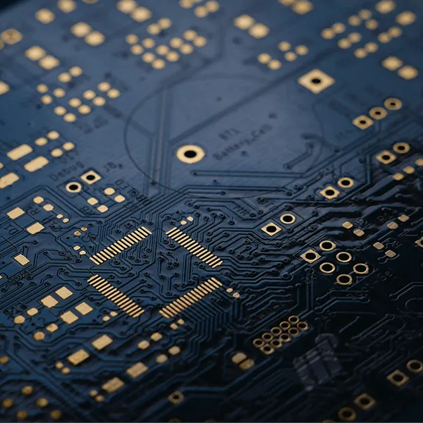
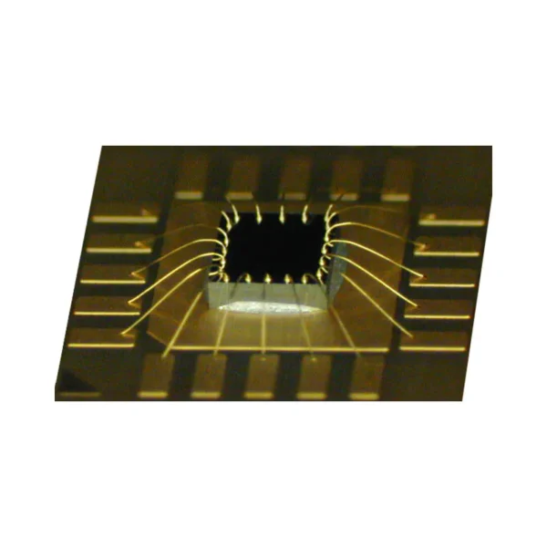
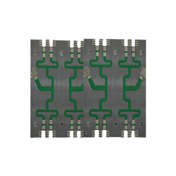
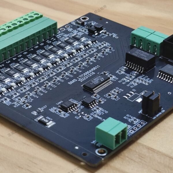
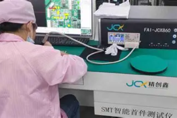
SysPCB has extensive experience in manufacturing PCBs and PCB assembly (such as component assembly and stencil). We are a professional Chinese PCB manufacturer and have served over 50 global clients for more than 16 years
SysPCB pcb manufacturing companies
Foreign Trade (Years)
Service Industry
Experienced Staff
Warranty Period(Days)
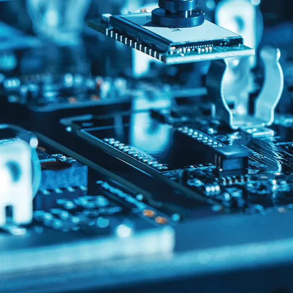
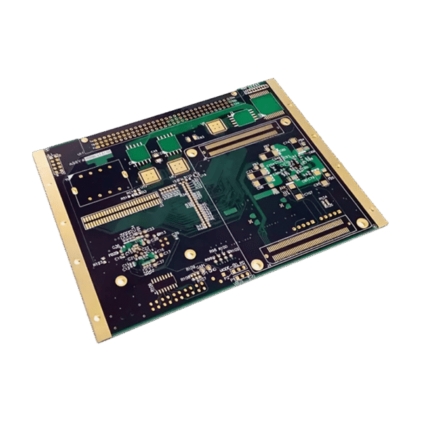
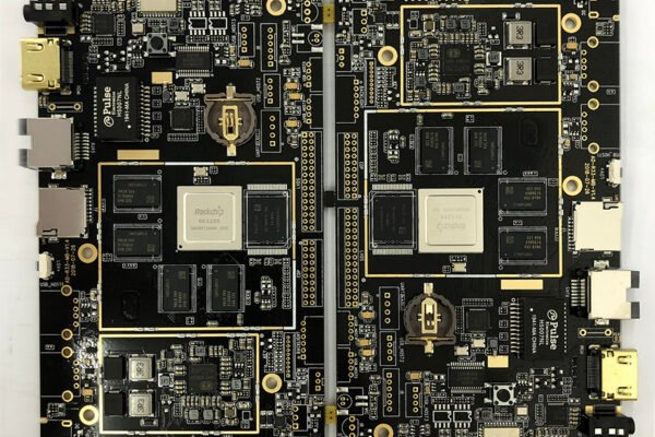
SysPCB provides PCB manufacturing and PCB assembly services, offering a one-stop solution to meet customer needs with greater flexibility.
China PCB Manufacturer with over 16 years of support for global customers

15% discount on price

Same Day-5 Day Delivery

International Standard

Professional Assembly
Professional PCB knowledge and news
To find out more information about our products and services, send us a message and one of our PV experts will get back to you. We look forward to assisting you via online live chat.
Contact Now