Heavy copper PCBs are mainly used in high-power distributors, heat sinks, planar transformers, and power ACs. We can produce Heavy copper PCBs up to 20oz. In general, if your circuit is going to pass a large current, it is recommended to choose a heavy copper circuit board. So what exactly is a heavy copper circuit board? Why choose heavy copper PCB for high current?
1. let’s talk about what is heavy copper PCB?
Everyone should know that the circuit board is made of copper clad laminate. There is a layer of copper foil on both sides of the copper clad laminate. When the thickness of the copper foil is greater than or equal to 2oz, the circuit board is defined as a heavy copper plate.
Heavy copper PCBs (Thick copper PCBs) are a special type of PCB. Its conductive materials, substrate materials, production processes, and application fields are all different from conventional PCBs. Plating of thick copper circuits allows PCB manufacturers to increase the copper weight in through-hole sidewalls and plated holes, which can reduce layer count and footprint. Thick copper plating integrates high current and control circuits, enabling high density with simple board construction.
2. What are the characteristics of heavy copper plate?
Copper realizes the effect of conducting electricity on the circuit board, and the heavy copper plate has the characteristics of carrying large current, reducing thermal strain, and good heat dissipation.
①. Heavy copper circuit boards can carry large currents
In the case of a certain line width, increasing the copper thickness is equivalent to increasing the cross-sectional area of the circuit, so that it can carry a larger current.
②. Heavy copper circuit board reduces thermal strain
Copper foil has a small conductivity, and the temperature rise is small when passing a large current, so the heat generation can be reduced, thereby reducing thermal strain.
Tip: The conductivity is the resistivity, and the metal “conductors” are divided into: silver→copper→gold→aluminum→tungsten→nickel→iron according to the conductivity.
③. Heavy copper circuit board has good heat dissipation

Heavy copper PCB stack up
Copper foil has high thermal conductivity (thermal conductivity 401W/mK), which can play an important role in improving heat dissipation performance.
Tip: Thermal conductivity refers to the heat transfer through 1m2 area within 1H for a material with a thickness of 1m and a surface temperature difference of 1°C on both sides under stable heat transfer conditions, and the unit is W/m•K.
The construction of thick copper circuits brings the following advantages to the PCB:
1. Greatly increase the current capacity
2. Higher thermal strain tolerance
3. Better heat dissipation
4. Increase the mechanical strength at the connector and PTH hole
5. Reduce product size
Table of Contents
Principle of Heavy Copper PCB:
⑴ Copper sinking process
Copper deposition is an important step in the manufacturing process of heavy copper PCBs. The purpose is to form a uniform copper layer on the substrate of a printed circuit board for conducting electricity and connecting electronic components. The specific process is as follows:
- Chemical deposition: Place the PCB, which has already been printed with circuit patterns on the substrate of the printed circuit board, into a chemical solution containing copper ions.
- Electrochemical reaction: Through electrochemical reaction, copper ions on the printed circuit board are reduced to metallic copper. During this process, copper ions will be adsorbed onto the cathode in the chemical solution and gradually form a uniform copper layer.
- Chemical reagents: Add some chemical reagents, such as surfactants and buffering agents, to regulate and control the speed and uniformity of chemical reactions, avoiding adverse phenomena such as uneven copper layers or the generation of bubbles.
")
⑵ Electroplating process
Electroplating is carried out on the basis of copper deposition, with the aim of increasing the thickness and uniformity of the copper layer. The specific steps include:
- Deburring: Before copper deposition, the PCB substrate undergoes a drilling process, which can easily produce burrs. Deburring technology must be used to solve this problem.
- Alkaline degreasing: Remove surface oil stains, fingerprints, oxides, etc., adjust the polarity of the pore wall substrate to facilitate subsequent adsorption of colloidal palladium.
- Micro etching: Remove the oxide on the surface of the board, roughen the surface, and ensure good adhesion between the subsequent copper deposition layer and the base copper of the substrate.
Heavy copper PCB process flow
The general process flow of heavy copper PCB includes: cutting, drilling, copper sinking, pattern transfer, pattern electroplating, etching, solder mask, characters, surface treatment, punching, final inspection, packaging and shipping.
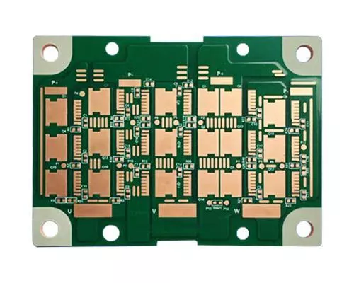
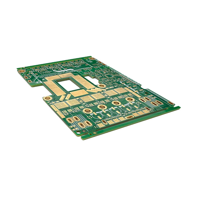
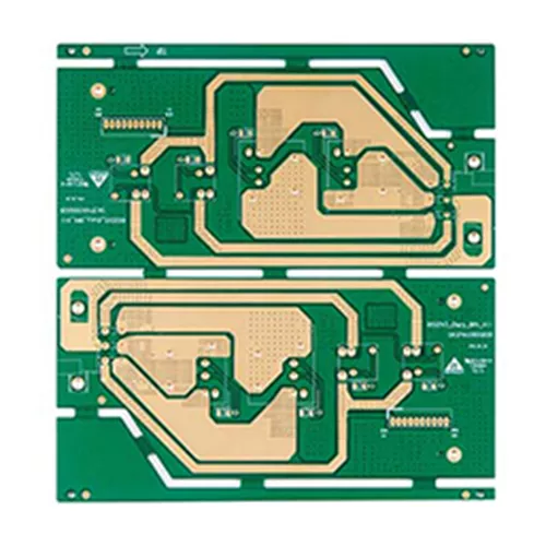
Application of thick copper PCB
With the increase of high-power products, the demand for thick copper PCBs has also greatly increased. Today’s PCB manufacturers pay more attention to the use of thick copper plates to solve the thermal efficiency problem of high-power electronic products. The application is as follows:
① Power electronic devices:
Thick copper PCBs can withstand higher currents and power, making them widely used in power modules, inverters, frequency converters, and other equipment.
② High frequency electronic devices:
Due to their low resistance and inductance, thick copper PCBs are commonly used in high-frequency electronic devices such as RF communication equipment, radar systems, microwave equipment, etc.
③ Automotive Electronics:
Automotive electronic devices need to withstand high temperatures and currents, and thick copper PCBs are used in engine control modules, electric vehicle chargers, and other applications due to their excellent heat dissipation performance.
④ LED lighting:
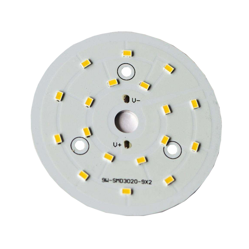
LED lighting products require high current and good heat dissipation performance, and thick copper PCBs are widely used in LED light strips, LED beads, and other products.
⑤ Industrial automation:
In industrial automation equipment, thick copper PCBs are commonly used in key parts such as motor drives and sensor interfaces. Their superior thermal conductivity and load-bearing capacity enable the equipment to maintain stability even under high loads.
⑥ New energy vehicles:
New energy vehicles have extremely high performance requirements for PCBs, especially in battery management systems and motor control systems. Thick copper PCBs have become an ideal choice due to their excellent electrical and heat dissipation performance.
⑦ Communication equipment:
In communication equipment, thick copper PCBs are used to achieve high-speed data transmission and signal processing, and their stable electrical performance ensures the stability and reliability of the equipment.

Heavy copper PCB microsection
Under the condition that other conditions remain unchanged, the calorific value of the line is inversely proportional to the thickness of the line. Therefore, designing the board as a heavy copper plate can reduce heat generation, thereby reducing thermal strain caused by heat generation.
To sum up, different from ordinary PCB, heavy copper plate has the significant advantages of carrying large current, good heat dissipation, and reducing thermal strain, which greatly reduces the risk of board burning, and is an excellent option for high-current PCB design. In addition, the design of heavy copper plate can also increase the mechanical strength of the circuit board and reduce the volume of the end product. With the development of science and technology, people need more and more electronic products with high performance, multiple functions, small size, capable of carrying large current and good heat dissipation, thus the demand for heavy copper plates is also increasing.
Based on the characteristics of the above heavy copper plate PCB, it is recommended that you choose a heavy copper plate for high current, which can better realize the circuit function.
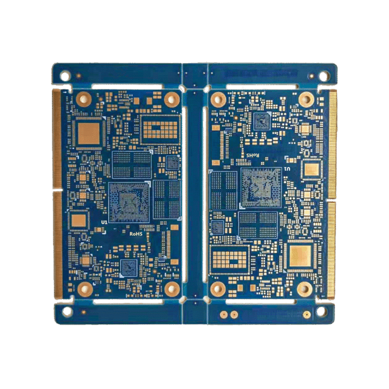
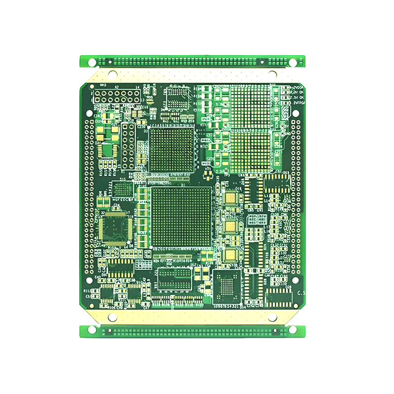
SYS Technology is a professional heavy copper circuit board supplier with rich manufacturing experience in the heavy copper PCB field, and supports heavy copper PCB proofing and mass production. Products can be widely used in mobile phones, microwave, aerospace, satellite communications, network base stations, hybrid integrated circuits, power high-power circuits and other high-tech fields. Multilayer heavy copper PCB production board factory, welcome to consult.
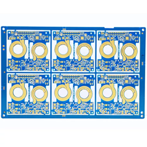
6 Layer Heavy copper PCB
Board thickness: 3.0mm
Copper thickness: 4/4/4/4/4/4oz
Application: Power supply
Max. current: 30A
Why choose SysPCB as the supplier of heavy copper PCB?
Heavy copper circuit PCBs play an irreplaceable role in PCB mass production applications with high power, high current and high cooling requirements. Heavy copper PCB manufacturing process and materials have higher requirements than standard PCB. SYS Technology has advanced equipment and professional engineers to provide high-quality thick copper PCBs for domestic and foreign customers.
Over 10 years of rich experience
SysPCB has over 10 years of experience in producing heavy copper PCBs. If you have any unsolvable problems in this area and want someone to help solve them, SysPCB can assist you, clarify your doubts, and manage the entire process for you. Its clear and transparent workflow helps save you time and energy. After placing the order, you only need to wait for the delivery of the goods.
Comprehensive Pre-Sales and After-Sales Support
SysPCB offers dedicated pre-sales support with a professional customer service and technical team available to assist with any inquiries or consultations at your convenience. Post-sales, we are committed to addressing any quality issues by offering rework services or appropriate compensation. Ensuring a positive customer experience is a core value of our company, and we strive to provide exceptional service at every stage of your engagement with us.
No MOQ
SysPCB does not have a minimum order quantity (MOQ) requirement, so you can confidently partner with us. As an Heavy Copper PCB manufacturer, we are committed to building long-term relationships based on mutual trust and benefit.
Due to economic development, the demand for heavy copper PCBs has increased, and they have been increasingly widely used in many applications; If you need heavy copper PCB manufacturing services, please feel free to contact our sales team at any time to obtain a heavy copper PCB quotation!