

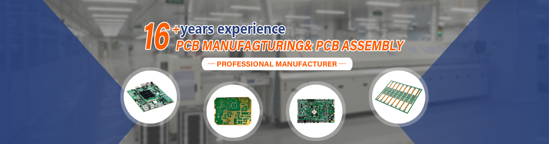
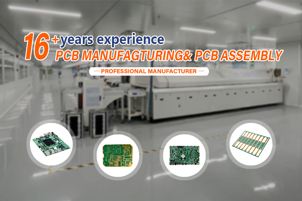
SMT Capability
| SMT Capability | ||||
| Item | Mass production(mm) | Sample&Small order(mm) | ||
| SMT PCB | Lenght*Width | Min. | 50*30 | L<50 or W<30 |
| Max. | 450*350 | 450<L≤800 or 350<400 | ||
| Thickness | Min. | 0.8 | T<0.8 | |
| Max. | 5 | T>5 | ||
| DIP PCB | Lenght*Width | Min. | 50*30 | L<50 |
| Max. | 500*300 | 500<L≤1000 or 300<W≤450 | ||
| Thickness | Min. | 0.8 | T<0.8 | |
| Max. | 5 | T>5 | ||
| Suface Mount Device | Size | Min. | 0603(0201) | 0402(01005) |
| Max. | 45*45 | 45*45<Size≤68*68(45*150) | ||
| Thickness | 25.4 | T>25.4 | ||
| QFP/SOP/SOJ/IC/Socket etc. | Min.PIN Distance | Pitch=0.4 | Pitch=0.3 | |
| CSP、BGA | Min.Tin ball Distance | Pitch=0.5 | 0.3≤Pitch<0.5 | |
| PCB Type | FR4、FPC、Rigid-Flex、PCB、Metal Core PCB | |||
What information is required for SMT processing at PCBA factory?
In SMT processing, the following information needs to be provided to the SMT factory during evaluation and quotation, so that engineers and procurement personnel can evaluate the process and quotation based on SMT Capability.
In PCBA SMT processing, if you need the supplier to provide one-stop PCBA processing service, then the communication and cooperation in the early stage need to be more adequate. The contract for labor and material service requires PCB board manufacturing information and assembly instructions, BOM list, Gerber information, etc. The lack of a certain item of information will cause an increase in communication costs and delays in delivery, which will have a very large impact on the timely launch of the product. So today we start from the SMT supplier’s angle of view, and analyze why we need relevant information:
1. Gerber data, (includes Pad layer, solder mask layer, silk screen layer, and paste layer)
It is a highly authoritative document in SMT processing, because the follow-up PCB quotation and assembly quotation all need Gerber files for reference. The stencil must be used for SMT processing, so the information of the stencil layer must be known when making stencil.
2. BOM list (component list)
It is what materials are included on a PCBA board. These corresponding materials have different brands, part numbers, and specifications, so the prices are also different, and the calculation of the assembling fee also needs to be evaluated based on the quantity of the components.

3. Coordinate file
It mainly locates the coordinates of the components, and the file is needed when SMT engineers make assembly program for the PCB project.
4. Process instruction document
For controlling the process in PCB assembly factory, it will generally contained as some guidance documents for the PCB manufacturer, including special needs and special design points.
5. Test instructions
There are various test items and categories, including test parameters and technical indicators, and abnormal on-site treatment methods.
The above 5 points are the information needed in SMT processing.
The main features of Surface Mount Technology
SMT process is now more and more mature for electronics manufacturing. What are the main features of SMT PCB Assembly process, today China SMT factory will introduce to you.
1. High density
Since the number of pins processed by SMT is as high as hundreds or even thousands, the center distance of the pins can reach 0.3mm. The high-precision BGA on the circuit board requires fine lines and fine spacing, and the line width is reduced from 0.2~0.3mm to 0.1mm or even 0.05mm, the double wire between the 2.54mm grid has developed to 4, 5 or even 6 wires. Thin lines and fine pitches greatly increase the assembly density of SMT.
2. Small aperture
Most of the metallized holes in SMT are not used to insert component pins, and no welding is performed in the metallized holes. The metallized holes are only used as electrical interconnections between layers, so the aperture should be reduced as much as possible to provide more space for the SMT. The aperture has changed from 0.5mm in the past to 0.2mm, 0.1mm and even 0.05mm.
3. Low thermal expansion coefficient
any material will expand after heating. Polymer materials are generally higher than inorganic materials. When the expansion stress exceeds the material bearing limit, the material will be damaged. Due to the many and short SMT pins, the CTE between the device body and the SMT is inconsistent, and device damage caused by thermal stress occurs from time to time. Therefore, the CTE of the SMT circuit board substrate should be as low as possible to suit the matching with the device.
4. Good high temperature resistance
Today, most circuit boards today need to install components on both sides. Therefore, SMT processed circuit boards need to be able to withstand two reflow soldering temperatures. At present, lead-free soldering is widely used, and the soldering temperature is higher. After soldering, the circuit board is required to have small deformation and no blistering, the pads still have good solderability, and the surface of circuit board still has a high flatness.
