


PCB Electric Test
What are the PCB testing methods
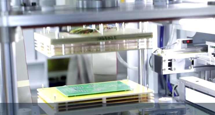
Dedicated to provide printed circuit boards that meet your expectations, SYS Tech is committed to carry out controls throughout the manufacturing process. This allows us to consistently deliver high quality PCBs that meet your specs. To pursue excellence, we regularly upgrade our production equipment, carry many in-process control and right at the end, before packing, we carry out an electrical test. 100% of all our PCB will go through this procedure. During this simple test, we will check 2 main types of defaults open circuits and shorts. Depending on customer’s requirement, we are also able to carry out other types of tests typically a tension of 400V, an impedance control, a dimension CPK, etc.
PCB board AKA printed circuit board is an important electronic component. The quality of PCB determines the quality of electronic products to a large extent. Therefore, in the process of producing PCB boards, inspection is a very important part. Through inspection, it is usually possible to find open circuit, short circuit and other defects that affect the function that are not easy to find visually.

For any designed product to be ultimately successful, it must be tested many times. PCB circuit board testing can minimize major problems, find smaller errors, save time and reduce overall costs.
PCB testing is primarily used to mitigate issues throughout the manufacturing process as well as the final production process. These types of tests can also be used on prototypes or small-scale assemblies, which can help identify potential problems that may exist in the final product.
Four testing methods of PCB bare board
01) PCB Testing-AOI test:
AOI automatic optical inspection equipment has been widely used in various industries. In the process of PCB manufacturing, as important inspection equipment, AOI test are also widely used.
AOI is also called mid-test in the PCB production process. It tests the circuit pattern after etching the copper foil on the PCB. The equipment scans the graphics on the board and compares it with the design documents, distinguishes the PCB surface graphics status, and then compares it with the PCB surface graphics data registered by the AOI itself. If there is a difference, the defect will be reported, and finally confirmed by the inspector.

02) PCB Testing-Flying probe test:
Flying probe testing is a well-recognized and effective form of testing for finding production quality issues, and flying probe testing has been proven by the industry to be a particularly cost-effective test method for circuit boards.
Flying probe tests use two or more independent probes and are run without fixed test points. These probes are electromechanically controlled and move according to specific software instructions. Therefore, the initial cost of the flying probe test is lower, and the test efficiency is not high compared with the fixture test. After all, the flying probe test is a point-by-point test of moving the probe, so it is practical for the test for small batch PCB orders.
03) PCB Testing–Fixture test:
The Fixture is a special jig designed for a particular PCB board for electrical performance on-off testing. There are single-sided jigs and double-sided jigs.
PCB electrical test first needs to make a set of test fixtures, connect the pads or test points on the PCB board through the metal probes of the fixture, and obtain the voltage value, current value and other typical values of the test circuit when the PCB board is powered on. So as to observe whetherthe tested circuit is connected normally. The advantage of using electrical testing is that the testing efficiency is high, and the disadvantage is that the cost is also high. Each PCB requires a different test fixture. Therefore, the fixture test is suitable for large-scale orders.
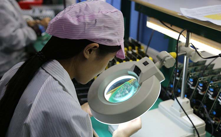
04) PCB Testing-Manual visual inspection:
Visual inspection is the most traditional inspection method, with the advantages of low initial cost and no test fixtures. Judge whether the pcb board is qualified by visual inspection using a magnifying glass or a calibrated microscope and determine when corrective action is required.
Visual inspection are only for boards with simple circuits, and the disadvantages are subjective human error, high long-term cost, discontinuous defect detection, and difficulty in data collection. As PCB production increases and shrinking of wire spacing and component volumes on PCBs, visual inspection methods are becoming less and less feasible.
Basic Principles of PCB Testing
By connecting metal probes to the pads and test points on the PCB and powering the PCB, standard parameters such as voltage and current are measured to verify product quality. Test fixtures are customized according to customer requirements and typically consist of an epoxy board, metal probes, wires, and detection interfaces to check circuit continuity and ensure no short circuits, disconnections, or open circuits.
Specific Testing Methods:
1. Solder Mask Hardness Test: A standard test pencil is used to scratch the PCB surface, and the minimum hardness is recorded to ensure the solder mask hardness exceeds 6H.
2. Ionic Contamination Test: An ion contamination tester measures the number of ions per unit area on the sample surface to ensure ion concentration is below a specified level.
3. Curing Test: Methylene chloride is dropped on the solder mask to check for dissolution or discoloration, verifying the solder mask’s resistance to chemical corrosion.
4. Thermal Stress Test: Strain gauges monitor deformation of the PCB during production to ensure strain remains within 500 µε.
Purpose and Significance of Each Test:
1. Solder Mask Hardness Test: Ensures the durability and stability of the solder mask.
2. Ionic Contamination Test: Prevents electrochemical effects on the PCB.
3. Curing Test: Assesses chemical resistance of the solder mask and markings.
4. Thermal Stress Test: Monitors PCB deformation during production to ensure product quality.
What are the PCBA tests?
The process of PCBA processing is very complicated, including PCB bare board process, component procurement and inspection, SMT, DIP, PCBA test and many other important processes. Because in the production process, there may be various problems due to improper equipment or operation, so can’t guaranteed the every products are qualified. Therefore, PCBA testing is required to ensure that each product does not have quality problems.
PCBA tests mainly include:
1. In circuit test mainly include circuit continuity, voltage and current values and fluctuation curves, amplitude, noise, and so on.
2. The function check test requires IC program burning, simulates the function of the entire PCBA board, finds problems in hardware and software, and equips the necessary production fixtures and test fixtures.
3. The aging test is mainly to energize the PCBA board and electronic products for a long time, maintain their work and observe whether there is any failure. After the aging test, the electronic products can be sold in batches.
4. The fatigue test is mainly to sample the PCBA board, and perform high-frequency and long-term operation of the function to observe whether there is a failure and judge the probability of the test failure, so as to feedback the working performance of the PCBA board.
5. Test in the harsh environment is mainly to expose the PCBA board to the limit temperature, humidity, drop, splashing, vibration, and obtain the test results of random samples, so as to infer the reliability of the entire PCBA board batch product.
PCBA Function Test
SYS Tech dedicated PCBA facility is fully equipped with state-of-the-art testing and verification equipment. Finished PCB Assemblies are checked for proper component placement and functionality with a variety of methods including AOI Inspection, In-Circuit testing, and X-Ray inspection.
The functional test for assembled circuit board is called FVT (Function Verification Test). The purpose of test is to pick up the poorly assembled board and test the whole function by simulating the circuit board.
This is to pick up the defective circuit board before assembling the machine, avoid occurring problem after whole machine assembled, also to avoid the waste of working labor and the loss of material.
ICT And Functional PCB Testing Ensure Quality
SYS Tech is highly process focused with an adherence to J-STD-001 standards. All PCB assemblies are verified for part-placement accuracy the use of critical checks such as signal integrity, functionality and performance to test specifications are fully incorporated into our PCBA testing procedures. Comprehensive PCBA testing capabilities include functional PCBA testing equipment and in-circuit testing (ICT).
What is ICT test for PCBA?
The full name of ICT is In—Circuit—Tester, it is a common PCBA test method in PCBA processing.
The ICT test mainly detects faults such as short circuits, open circuits, and component soldering by contacting test points on the PCBA board with test probes. Capable of quantitatively measuring resistance, capacitance, inductance, crystal and other components, functional tests on diodes, triodes, optical amplifiers, transformers, relays, operational amplifiers, power modules, etc., and functional tests on small and medium-sized integrated circuits, such as 74 series, memory class, common driver class, exchange class IC.

Common ICT test methods
1. Analog device test
Test with operational amplifers. The concepts of “virtual ground” from point “A” are:
∵Ix = Iref
∴Rx = Vs/ V0*Rref
Vs and Rref are the excitation signal source and the instrument’s calculated resistance, respectively. Measure V0, then Rx can be found. If the Rx to be measured is a capacitor or an inductor, the Vs AC signal source and Rx are in the form of impedance, and C or L can also be obtained.
2. Vector test
For digital ICs, the Vector test is used. The vector test is similar to the truth table measurement, stimulating the input vector, measuring the output vector, and judging the quality of the device through the actual logic function test. Example: NAND gate test.
For the test of analog IC, the voltage and current can be stimulated according to the actual function of the IC, and the corresponding output can be measured as a function block test.
3. Non-vector testing
With the development of modern manufacturing technology and the use of very large-scale integrated circuits, it often takes a lot of time to write a vector test program for the device. For example, the test program of the 80386 requires a skilled programmer for nearly half a year. The large number of applications of SMT devices has made the open pin fault phenomenon more prominent. To this end, various companies launched the non-vector testing technology, for example, Teradyne launched MultiScan, GenRad launched Xpress non-vector testing technology.
ICT testing is at the back end of the PCBA production process but it is the first process of PCBA testing, can timely discover problems in the PCBA board production process, which helps to improve the process and increase the production efficiency.
PCBA testing includes five main types: ICT test, FCT test, Aging test, Fatigue test, and test in harsh environment.
1. ICT test mainly includes the open/short of the circuit, the voltage and current value and the fluctuation curve, the amplitude, the noise and so on.
2. FCT test, need burn in IC program first, the function of the whole PCBA board is simulated and tested, the problems in hardware and software are found.
3. Fatigue test is mainly about sampling the PCBA board, performing high frequency and long time operation, observing whether there is failure, judging the probability of failure, so as to estimate the working performance of PCBA board in electronic products.
4. Test in harsh environment, testing the PCBA board exposed to high temperature, humidity, drop, splash and vibration, and the reliability of the whole PCBA batch is deduced.
5. The aging test is mainly to power the PCBA board or electronic products for a long time, maintain its work and observe if any failure occurs. After aging test, the electronic products can be sold in batch.

What does the functional test contain?
1. Power testing. Test power supply of PCBA, test individual point voltages using hysteresis comparator etc.
2. Open/short test for port/interface.
3. IC module read and write functional test.
4. Special function testing (different PCBA testing requirements are different), for example, PCBA with infrared function, external receivers are required for testing.
ICT and FCT, this two testing methods are very different, not only because the ICT equipment and tools are relatively expensive, but it can give good test results and bring convenience to rework.
Principles of PCBA Functional Testing
Using an FCT test fixture to connect test points on the PCBA, a complete circuit pathway is formed, linking to a computer and a programmer to upload the MCU program onto the PCBA. During testing, the MCU program captures user input actions (e.g., holding a switch for 3 seconds) and, through computations, controls the adjacent circuit’s on/off states (e.g., flashing an LED or activating a motor). By observing the voltage and current values between test points on the FCT fixture and verifying these inputs and outputs align with the design, the entire PCBA board is tested.
Specific Steps and Methods of PCBA Functional Testing:
1. Current Testing: Checks for current leakage issues on the board; if the current is below the design threshold, the test passes.
2. Voltage Testing: Tests the board’s withstand voltage by gradually increasing voltage; if no faults occur, the test passes.
3. Corrosion Resistance Testing: Applies a specific liquid to the board for a set period; if appearance and function remain normal, the test passes.
4. Heat and Humidity Resistance Testing: Simulates high-temperature and high-humidity conditions; if the board functions normally and maintains its structure over a certain period, the test passes.
5. Vibration Testing: Places the board on a vibration device for a specified time; if functionality, structure, and component soldering remain intact, the test passes.
6. Impedance Testing: Uses an ohmmeter to verify that the impedance values of circuits or components fall within specified ranges.
PCBA manufacturing process is complex. In the process of production and processing, there are maybe a variety of problems due to improper equipment or operation. Nobody can ensure that the products produced are qualified. Thus, it is necessary to carry out PCBA testing in order to ensure that each product does not exist quality problems.
PCBA aging testing
The purpose of the aging test is to simulate the daily use environment of the product, thereby exposing PCBA defects, such as poor soldering, mismatching component parameters, and failures during debugging etc., so as to eliminate and improve defect-free PCBA boards and stabilize parameters. Today, China PCBA factory SysPCB will introduce the standard of aging test.
The aging test of PCBA is carried out through the combined effect of high temperature, low temperature, high and low temperature changes and electric power.
PCBA Aging Test Standard:
1. Low temperature work
After placing the PCBA board at a temperature of -10±3°C for 1 hour, under this condition, with rated load, power on and run all programs, and the program should be correct.
2. High temperature work
After placing the PCBA board at 80±3℃ for 1h, under this condition, with load, power on and run all programs, and the programs should be correct.
3. High temperature and high humidity work
Put the PCBA board under the conditions of temperature 65±3℃, humidity 90-95%, time 48h, power on and run each program with rated load, and each program should be correct.
PCBA aging testing equipment
The specific practices of the PCBA aging test are:
1. Place the PCBA board at ambient temperature into the heat aging equipment at the same temperature, and the PCBA board is in operation.
2. Reduce the temperature inside the equipment to the specified temperature at a specified rate. After the temperature in the equipment has stabilized, the PCBA board should be exposed to low temperature for 2 h.
3. Increase the temperature inside the equipment to the specified temperature at a specified rate. After the temperature in the equipment has stabilized, the PCBA board should be exposed to high temperature for 2 h.
4. Reduce the temperature inside the equipment to room temperature at a specified rate, repeat until the specified aging time, and measure and record the PCBA board according to the specified aging time.
About SysPCB
We are a reliable Chinese PCB manufacturer, dedicated to becoming a long-term partner for our customers. We provide reliable PCB production services to ensure a high level of cooperation with customers in terms of quality, delivery time, and after-sales support.