Table of Contents
What Is A Multilayer Board?
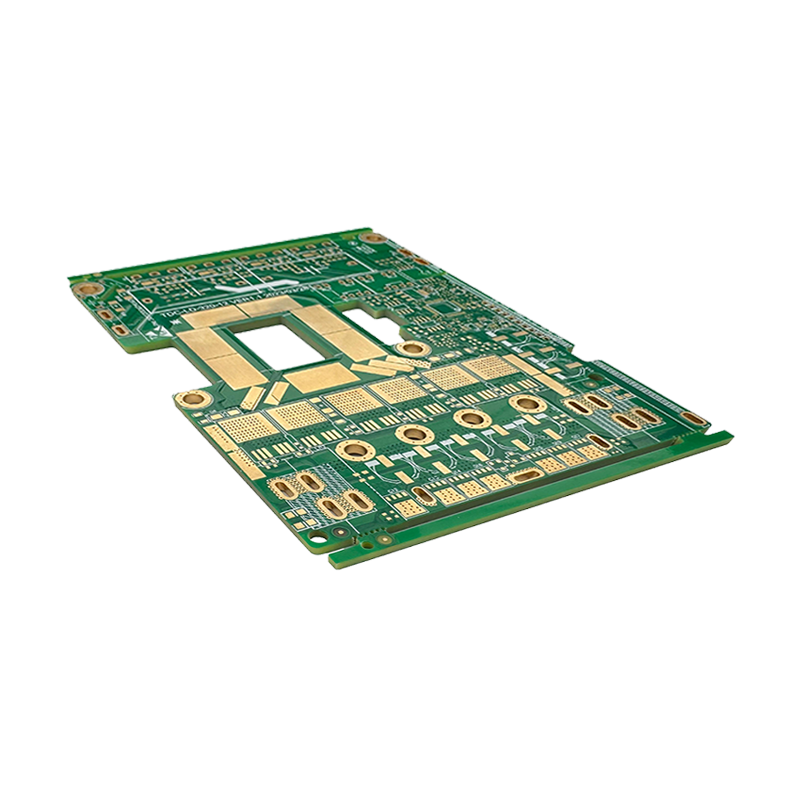
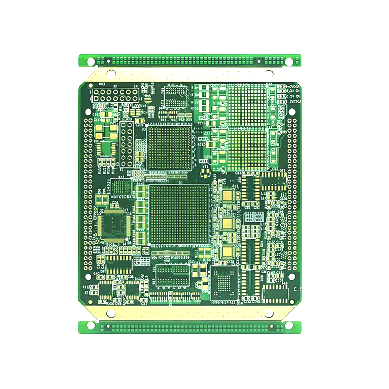
Multilayer PCB is a PCB with more than three conductive pattern layers and insulating material laminated between them. Multilayer PCB have multiple circuit layers, two of which are on the outer surface, and between each of the two layers is a dielectric layer. The dielectric layer can be made very thin, so the thickness of the multilayer PCB can be made just as thin as that of the double sided PCB. The electrical connections between them are usually made through plated through holes in the cross section of the board. Currently, SYS Technology is able to produce up to 64 layers.

In this article we take a closer look at multilayer PCB, including the following:
- Application Areas for Multilayer PCB
- Multilayer PCB Manufacturing Process
- Precautions for producing multi-layer PCB
- Common Multilayer PCB Stack-up
- SYS Technology’s Efforts to Make Reliable Multilayer PCB
- Application Areas for Multilayer PCB
With the development of technology, multilayer PCB have become an integral part of modern electronic devices. It can achieve higher signal transmission efficiency and higher functional density by designing multiple circuit layers on the same board. This performance makes multilayer PCB widely used in various applications.
1. Communications
Multilayer PCB has a wide range of applications in the field of communications. For example, the motherboard used in mobile phones is a multilayer PCB. Mobile devices need to integrate multiple components, including processors, memory, communication modules, etc., in a very limited space. Multilayer PCB can meet these requirements and also provide faster data transfer speeds and more stable signal transmission.

2. Industrial control
Multilayer PCB circuit boards are also widely used in industrial automation control systems. These systems typically require high-speed data transmission and complex control logic, and they also need to operate under harsh environmental conditions. Multilayer PCB can provide higher anti-interference ability and reliability, making industrial control systems more stable and reliable.

3. Medical devices
Medical equipment requires highly precise electronic control and signal processing, which requires circuit boards to have higher performance and stability. Multilayer PCB can achieve more complex functional integration and provide higher data transmission speed and anti-interference ability, making medical equipment safer and more reliable.

4. Aerospace
Multilayer PCB also plays an important role in the aerospace sector. For example, circuit boards used in flight control systems must have extremely high reliability and anti-interference capabilities to ensure the safety of aircraft. Multilayer PCB circuit boards can achieve higher signal transmission efficiency and higher reliability, making flight control systems safer and more reliable.
5. Automotive Electronics
With the development of automotive electronics, multilayer PCB has gradually become an integral part of automotive electronics. For example, the circuit boards used in in-car entertainment systems must have high-speed data transmission and complex control logic, but also need to work in harsh environmental conditions. Multilayer PCB can provide higher anti-interference capability and higher reliability, making the in-car entertainment system more stable and reliable.
In summary, multilayer PCB have a wide range of applications in the fields of communications, industrial control, medical devices, aerospace and automotive electronics. With the continuous development of science and technology, the application areas of multilayer PCB will also become more and more extensive.
Multilayer PCB Manufacturing Process
PCB factories do not directly manufacture copper-clad laminates, semi-cured sheets, copper foils and other substrates, but rather to the upstream of the industrial chain of substrate manufacturers to purchase the required substrate, the substrate in the factory are standard large size, such as 1mx1m (or 1mx1.2 m) specifications. Then before the PCB is manufactured, it needs to be cut to the size required for the production line according to the specifications of its own processing equipment.
After cutting, for the process of multilayer boards, the first production of the inner layer of the circuit, such as the inner layer of graphic production, Lamination and other processes, and then the process is back to the same process with the double-layer boards, such as drilling, plating, the outer layer of graphic production, and so on, and finally all kinds of testing and packaging shipment.
Taking our SYS Technology as an example, the specific production process for multi-layer PCB can be refined to the following 33 steps:

Multi-layer board production process
The specific operations for each step above can be viewed in the PCB Manufacturing Overview.
Precautions for producing multi-layer PCB
With the development of electronic technology to high-speed, multi-function, large capacity and portable low-consumption direction, the application of multi-layer PCB is more and more widely, and its layer number and density are also higher and higher, and the corresponding structure is also increasingly complex. The production of multilayer PCB has become the most important part of the whole PCB industry. The emergence of multi-layer board technology is a major development of PCB industry, which makes the whole PCB technology advance by leaps and bounds.
So what precautions should we pay attention to when producing multi-layer circuit boards?
1. Lamination
All multi-layer boards must have a lamination process. During this process, if you do not pay attention, delamination, slippery boards and other phenomena will occur. Therefore, the performance of the material must be considered in the design. The more layers there are, the more difficult it is to control expansion and contraction, as well as compensate for size coefficients, which leads to problems. If the insulation is too thin, test failures may occur. Therefore, more attention is paid to the lamination process, where more problems at this stage.
2. Inner layer lines
The materials used to manufacture multilayer boards are also very different from other boards. For example, the copper skin on the surface of the multilayer board is thicker. This makes it more difficult to lay out the inner lines. If the inner core board is thin, it is prone to abnormal exposure, which may be caused by wrinkles. Generally speaking, the unit size of multilayer boards is relatively large, and the production cost is very high. Once problems arise, it will bring huge losses to the business.

3. Alignment
The more layers there are, the higher the interlayer alignment requirement will be. Generally speaking, the interlayer alignment tolerance is controlled at ±75 μ M. Due to the influence of dimensions, temperature and other factors, the difficulty coefficient of interlayer alignment manipulation of multilayer boards can be very large.
4. Drilling
The difficulty of drilling is also increased because the multilayer boards are made of special materials. It is also a test of drilling technology. Due to the increased thickness, the drilling tools are easy to break and a series of problems such as oblique drilling may occur. We should pay more attention to it!
Common Multilayer PCB Stack-up
High assembly density, small size, and light weight are the advantage of multilayer PCB. Due to the high assembly density, the circuits between components is reduced, thereby improving reliability; more layers can be used, thereby increasing design flexibility; could design impedance control circuit; a high-speed transmission circuit can be formed; magnetic circuit shielding layer can be set, and a metal core heat dissipation layer can also be set to meet the needs of special functions such as shielding and heat dissipation; simple installation and high reliability.
Let’s take a look at the stack-up of common multi-layer PCB:
4 layers laminated stack-up


6 layers laminated stack-up

8 layers laminated stack-up


10 layers laminated stack-up

SYS Technology’s efforts to produce high-quality and reliable multilayer PCB
The manufacturing of high-layer, high-difficulty, special materials, special process circuit boards, which has always been our characteristics, the continuous improvement of high-multi-layer circuit board manufacturing process as our goal.
Every year we invest a lot of human resources and material resources in production equipment and process research and development and try our best to catch up with the development of cutting-edge circuit board manufacturing technology.
SysPCB is committed to solving customers’ pain points for difficult boards, precision boards, and special boards with nowhere to process, improving the high reliability of products, effectively avoiding process defects, and ultimately meeting customers’ quality requirements.
I: CCL selection
The quality of raw materials directly affects the quality of printed circuit boards. Therefore, in order to improve the high reliability of HDI, the SysPCB strictly selects Shengyi A-level CCL, which provides a basic guarantee for product quality.
II: Press equipment
High-performance pressure machines can meet the accuracy and reliability of interlayer alignment of high-end boards. The SysPCB introduced the German BURKLE vacuum laminator and other supporting equipment to form a lamination line for high-precision multi-layer PCB lamination.
III. Drilling process
The traditional mechanical method can no longer meet the drilling requirements. SysPCB is equipped with superior processing capacity, improves productivity, achieves stable processing quality and high processing positioning accuracy.
For the multi-layer boards required by the market, the advantages of the SysPCB are as follows:
- Up to 64 layers;
- Back-drilling can reduce the loss of signal transmission;
- Aperture ratio 15:1, plate thickness 0.4-10.0mm;
- Blind hole technology, impedance control;
- The alignment deviation between layers can be controlled within 35um;
- Adopt a special design method – ventilation hole design to improve the bonding force between the copper layer and the hole wall.
- In addition, our inner layer connection quality control method can improve the process parameters and special parameters, so as to improve the inner layer connection quality.
SysPCB continuously optimizes the process level and improves the manufacturing capacity, and is committed to providing customers with high-reliability multi-layer board manufacturing services.
Hot tags: Multilayer PCB, multilayer circuit board, pcb solder mask, pcb board design, printing circuit boards, multi layer pcb board, multi layer printed circuit board, circuit board pattern, pcb keyboard, multilayer printed circuit board, Customized, cheap, quotation, suppliers, factory, manufacturer, manufacturing, manufacturing services