Table of Contents
What is Ceramic PCB?
Ceramic PCB refers to a special process board in which copper foil is directly bonded to the surface of alumina (Al2O3) or aluminum nitride (AlN) ceramic substrate (single-sided or double-sided) at high temperature. The ultra-thin composite substrate produced has excellent electrical insulation performance, high thermal conductivity, excellent brazing performance, and high adhesion strength. It can also etch various patterns like other FR4 PCB boards, and has great current carrying capacity. Therefore, ceramic substrates have become the fundamental material for high-power power electronic circuit structure technology and interconnection technology.
| Material parameters | unit | 96%AI2O3 | 99.6%AI2O3 | 96%AIN | SiC | Si3N4 | ZrO2 | ZTA | Piezoelectric ceramics | sapphire | diamond | Testing standards |
| colour | / | white | white | grey | grey | grey | white | white | Light yellow/Dark brown | transparent | faint yellow | / |
| bulk density | g/cm3 | ≥3.7 | 3.9 | ≥3.33 | 3.1-3.15 | ≥3.22 | ≥6.0 | ≥4.1 | 7.7 | ≥3.86 | 3.42-3.52 | GB/T 2413 |
| Warpage | ‰ | ≤2 | ≤2 | ≤2 | ≤2 | ≤3.18 | ≤4 | ≤4 | ≤2 | / | / | / |
| Surface roughness | μm | 0.2-0.75 | 0.05-0.1 | 0.2-0.6 | 0.2-0.4 | 0.2-0.4 | 0.1-0.2 | 0.1-0.2 | 1.6-6.4 | 0.05-0.08 | 0.02-0.002 | GB/T 6062 |
| thermal conductivity | 20℃ W/(m.K) | ≥24 | 29 | ≥170 | ≥100 | ≥20 | ≥3 | ≥27 | 2.5-3.5 | ≥26 | 1400-1850 | GB/T 5598 |
| Thermal expansion coefficient | 20-800℃ x106/K | 6.5-8.0 | 6.5-8.2 | 2.0-3.5 | 4 | 3 | 7.8 | 8 | 4.0-4.3 | 7.2 | 1-1.5 | GB/T 5593 |
| dielectric constant | 1MHz | 9-10 | 9-10.5 | 8-10 | / | 8-10 | 33 | 10.4 | 2.1 | 9.6-10.2 | 5.6 | GB/T 5594.4 |
| breakdown voltage | KV/mm | ≥17 | ≥17 | ≥17 | / | ≥14 | ≥10 | ≥10 | 24-30 | / | ≥10 | GB/T 5593 |
| Volume resistivity | 20℃ Ω·cm | ≥10-14 | ≥10-14 | ≥10-13 | / | ≥10-14 | ≥10-13 | ≥10-14 | ≥1012 | ≥10-14 | ≥10-14 | GB/T 5594.5 |
| bending strength | MPa | ≥350 | 450 | ≥330 | ≥400 | 980 | ≥800 | ≥650 | 1200 | ≥550 | ≥450 | GB/T 5593 |
Background technology of Ceramic PCB:
With the gradual deepening of electronic technology in various application fields, highly integrated circuit boards have become an inevitable trend. Highly integrated packaging modules require a good heat dissipation bearing system, while the disadvantage of traditional circuit boards FR-4 and CEM-3 in TC (thermal conductivity) has become a bottleneck restricting the development of electronic technology.
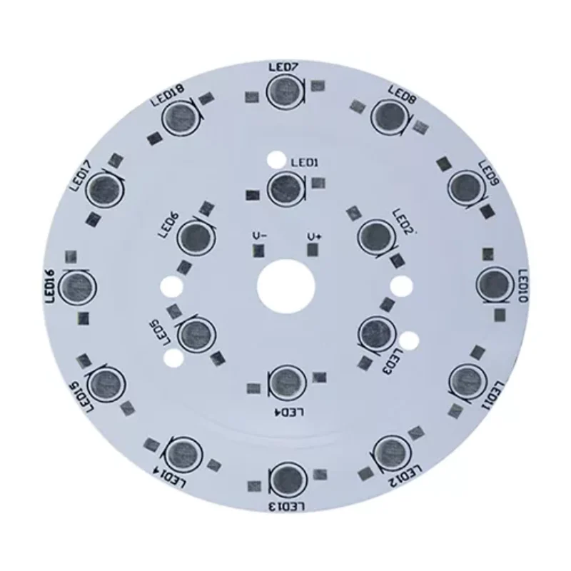
In recent years, the rapidly developing LED industry has also put forward higher requirements for its TC index for carrying circuit boards. In the field of high-power LED lighting, materials with good heat dissipation performance such as metals and ceramics are often used to prepare circuit substrates. The thermal conductivity of high thermal conductivity aluminum substrates is generally 1-4W/M. K, while the thermal conductivity of ceramic substrates can reach around 220W/M. K depending on their preparation method and material formula.

Features of Ceramic PCB:
- Strong mechanical stress and stable shape; High strength, high thermal conductivity, and high insulation; Strong adhesion and corrosion resistance.
- Good thermal cycling performance, with 50000 cycles and high reliability.
- A structure that can etch various shapes like a PCB board (or IMS substrate); Non polluting and pollution-free.
- Operating temperature range -55 ℃ to 850 ℃; The coefficient of thermal expansion is close to that of silicon, simplifying the production process of power modules.
Main advantages — Ceramic PCB:
Unlike traditional FR-4 (wave fibers), ceramic materials have excellent high-frequency and electrical properties, as well as high thermal conductivity, chemical stability, and thermal stability that organic substrates do not possess. They are ideal packaging materials for the new generation of large-scale integrated circuits and power electronic modules.
1. Higher thermal conductivity
2. More matching coefficient of thermal expansion
3. A stronger and lower resistance metal film layer. 4. The substrate has good weldability and high usage temperature
5. Good insulation
6. Low high-frequency loss
7. Can be assembled with high density
8. It does not contain organic components, is resistant to cosmic rays, has high reliability in aerospace, and has a long service life
9. The copper layer does not contain an oxide layer and can be used for a long time in a reducing atmosphere.
Disadvantages of Ceramic PCB:
1. Fragile: This is one of the main drawbacks, at present, only a small area of the board can be made.
2. The price is expensive: the requirements of electronic products are more and more, the ceramic circuit board is only satisfied to meet some of the more high-end products, the low-end products will not be used at all.
Performance requirement:
(1) Mechanical properties
- Having sufficient mechanical strength, it can be used as a supporting component in addition to carrying components;
- Good processability and high dimensional accuracy;
- Easy to achieve multi-layer;
- Smooth surface, without warping, bending, microcracks, etc.
(2) Electrical properties
- High insulation resistance and insulation failure voltage;
- Low dielectric constant;
- Low dielectric loss;
- Stable performance under high temperature and humidity conditions, ensuring reliability.
(3) Thermal properties
- High thermal conductivity;
- Matching the thermal expansion coefficient with relevant materials (especially with the thermal expansion coefficient of Si);
- Excellent heat resistance.
(4) Other properties
- Good chemical stability;
- Easy to metallize, circuit graphics have strong adhesion to them;
- No hygroscopicity;
- Oil and chemical resistance;
- The amount of radiation emitted is small;
- The substances used are pollution-free and non-toxic;
- The crystal structure remains unchanged within the temperature range of use;
- Rich raw materials;
- Mature technology;
- Easy to manufacture;
- The price is low.
Classification of Ceramic PCBs:
First, according to the material
1、 Al2O3
Alumina substrate is the most commonly used substrate material in the electronics industry because of its high strength and chemical stability compared to most other oxide ceramics in terms of mechanical, thermal and electrical properties, as well as a rich source of raw materials, suitable for a wide variety of technical manufacturing and different shapes.
2、BeO
It has a higher thermal conductivity than aluminum, and is used in applications that require high thermal conductivity, but it decreases rapidly after the temperature exceeds 300°C, and most importantly, its toxicity limits its development.
3 、AlN
AlN has two very important properties worth noting: one is the high thermal conductivity and the other is the coefficient of expansion that matches the Si. The disadvantage is that even a very thin oxide layer on the surface can have an effect on the thermal conductivity, and only a tight control of the material and process can make a consistent AlN substrate. However, with the improvement of the economy and the upgrading of technology, this bottleneck will eventually disappear.
Based on the above reasons, it can be known that alumina ceramics are still in a dominant position in the fields of microelectronics, power electronics, hybrid microelectronics, and power modules due to their superior comprehensive properties.
Second, according to the manufacturing process to divide
At this stage, there are five types of ceramic heat dissipation substrates: HTCC, LTCC, DBC, DPC, and LAM, and HTCCLTCC are all sintering processes, and the cost will be higher.
DBC and DPC are the domestic development in recent years, and the professional technology of energy production, DBC is the use of high temperature heating to combine Al2O3 and Cu plate, its technical bottleneck is not easy to solve the problem of microporosity between Al2O3 and Cu plate, which makes the mass production energy and yield of the product are greatly challenged, and DPC technology is the use of direct copper plating technology, Cu is deposited on the Al2O3 substrate, the process combines materials and thin film technology, and its products are the most commonly used ceramic heat dissipation substrates in recent years.
However, its material control and process technology integration capabilities are required, which makes the technical threshold for entering the DPC industry and stable production relatively high. LAM technology is also known as laser rapid activation metallization technology.
1、HTCC (High-Temperature Co-fired Ceramic)
HTCC is also known as high-temperature co-firing multi-layer ceramics, the manufacturing process is very similar to LTCC, the main difference is that the ceramic powder of HTCC is not added to the glass material, therefore, HTCC must be dried and hardened into a green embryo under a high temperature of 1300~1600 °C, and then the conduction hole is also drilled, and the hole is filled and printed with screen printing technology, because of its high co-firing temperature, the choice of metal conductor materials is limited, and its main materials are tungsten, molybdenum, manganese… and other metals, and finally laminated and sintered to form.
2、 LTCC (Low-Temperature Co-fired Ceramic)
LTCC, also known as low-temperature co-fired multilayer ceramic substrate, this technology must first mix inorganic alumina powder with about 30%~50% The glass material is added with an organic binder to make it evenly mixed into a muddy slurry, and then the slurry is scraped into a sheet by a scraper, and then the sheet slurry is formed into a thin embryo through a drying process, and then drilled through holes according to the design of each layer, as the transmission of signals in each layer, LTCC internal circuit is used screen printing technology, respectively, to fill holes and print circuits on the raw embryo, and the inner and outer electrodes can be used silver, copper, gold and other metals respectively, and finally each layer is laminated and placed in 850~It can be sintered in a sintering furnace at 900°C.
3、 DBC (Direct Bonded Copper)
The basic principle is to introduce an appropriate amount of oxygen between copper and ceramics before or during the laying process, in the range of 1065 °C ~ 1083 °C, copper and oxygen form Cu-O eutectic solution, DBC technology uses the eutectic solution to generate CuAlO2 or CuAl2O4 phase with the ceramic substrate on the one hand, and infiltrates the copper foil to realize the combination of ceramic substrate and copper plate.

Why use ceramic circuit boards?
Ceramic circuit boards are actually made of electronic ceramics and can be made into various shapes. Among them, ceramic circuit boards have the most outstanding characteristics of high temperature resistance and high electrical insulation performance, and have the advantages of low dielectric constant and dielectric loss, high thermal conductivity, good chemical stability, and similar thermal expansion coefficient of components.
Ceramic circuit boards are produced using LAM technology, a laser rapid activation metallization technology. Used in the following fields:
- High-power power semiconductor module, semiconductor cooler, electronic heater, power control circuit, power hybrid circuit.
- Intelligent power components, high-frequency switching power supplies, solid state relays.
- Automotive, aerospace and military electronic components.
- Solar panel components, telecommunication private exchanges, receiving systems, lasers and other industrial electronics.
SysPCB: A reliable manufacturer of Ceramic PCBs
With the advancement of technology, ceramic circuit boards will not only reach new heights in thermal conductivity, insulation, mechanical strength and other performance aspects, but also develop towards smaller sizes and higher integration to meet the market’s demand for miniaturization and efficiency of electronic devices. Therefore, there are certain requirements for the production technology and machinery of PCB manufacturers. You need reliable ceramic PCB suppliers to provide you with ceramic PCB services, SysPCB is your choice. The following are the advantages of our ceramic PCB manufacturing.
Over 10 years of Ceramic PCB manufacturing experience
We have over 10 years of experience in manufacturing ceramic PCBs. Due to the customer’s demand for ceramic PCB boards, we are very familiar with the manufacturing of ceramic core PCBs, which enables us to provide customers with more convenient and professional services.
No MOQ
We specialize in producing small to medium-sized ceramic PCBs. Our manufacturing capabilities allow us to tailor production to meet your order volume requirements, offering you efficient and flexible production services.
On-Time Delivery
As a dedicated ceramic PCB manufacturer, we are committed to delivering your orders within the agreed timeframe, ensuring you receive your ceramic core PCBs promptly for seamless integration into your subsequent projects.
Good quality
We have modern equipment and a professional team to ensure the excellent quality of ceramic core PCBs. After production and manufacturing, they can meet the requirements of customers, allowing them to place orders with us with confidence.