


What is impedance Impedance Controlled PCBs?
The impedance Impedance Controlled PCBs results from the interaction of reactance and resistance. It measures the resistance to current when an alternating current is applied to it. As an AC characteristic, impedance is frequency dependent and is expressed in ohms (Ω).
Its transmission is ideal whenever a signal passes through a conductor with the same impedance as another given impedance. The signal is affected if the impedances at the two ends are different.
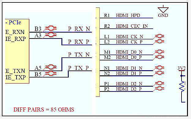
Impedance control is often required in single-ended microstrip, embedded microstrip, ribbon differential pairs, and planar PCB transmission lines.
How is impedance determined?
Impedance usually ranges from 25 to 125 ohms and depends mainly on the following factors.
- Width and thickness of the copper wire
- Signal path
- Core thickness or material thickness on both sides of the line
- The dielectric constant of the core or material
- Distance from the copper plane
- Presence of solder resist
Circuit board designers need to realize that their choice of conductors will directly affect the target impedance value. Many advanced tools are available to help with this calculation, which we will discuss later in the article.
Impedance matching is very important in realizing high-frequency design and is closely related to the quality of the signal. The purpose of impedance matching is mainly that all high-frequency microwave signals on the transmission line can reach the load point, and there will be no signal reflecting back to the source point.
SysPCB talk about PCB circuit board why do impedance control?
The impedance of the PCB board refers to the resistance and the parameters of the reactance, it acts as a hinder the AC. Impedance control is essential in the production of PCB boards. The reasons are as follows:

1. The PCB circuit board should be considered for mounting of electronic components. After mounting, the conductive performance and signal transmission performance should be considered. Therefore, the impedance control should be as low as possible, and the resistivity should be less than per square centimeter 1 times 10 to the negative six powers.
2. In the production process, the impedance circuit board must undergo the process of PTH (Plated Through Hole), HAL (Hot Air Leveling), soldering of the connector, etc., and the materials used in these processes must ensure low resistivity, then in order to ensure that the overall impedance of the circuit board is low, it meets the product quality requirements and can operate normally.
3. The tin-plating of the impedance circuit board is the most prone to problems in the whole circuit board production, and is the key process affecting the impedance board. The biggest defect of the electroless tin plating layer is that it is easy to change color (both easy to oxidize or deliquesce), and the soldering property is poor, which may cause the PCB board to be difficult to solder, the impedance is too high, and the conductivity is poor or the performance of the whole board is unstable.
4. There are various signal transmissions in the conductors in the impedance circuit board. When the transmission rate is increased, the frequency must be increased. If the line itself is different due to etching, stack thickness, wire width, etc., the impedance value will change and the signal will be distorted, resulting reduce the performance of the PCB. Therefore, it is necessary to control the impedance value within a certain range.
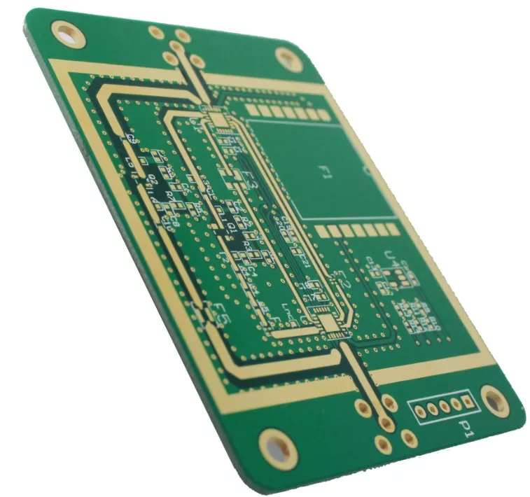
Functions of Multilayer Impedance PCBs
Multilayer impedance PCBs are PCBs with three or more conductive layers, separated by insulating materials and interconnected by vias. In such structures, precise impedance control of each signal line is essential, with the main functions highlighted as follows:
1. Improving Signal Integrity:
By precisely controlling the impedance of each signal line, reflections and crosstalk during transmission are effectively reduced, ensuring signal clarity and stability—crucial for high-speed signal transmission.
2. Increasing Circuit Density:
The multilayer structure allows designers to fit more circuits in limited space while maintaining good signal quality, which is a significant advantage for miniaturized, high-integration electronic products.

3. Optimizing Power Distribution:
Multilayer boards can have dedicated power and ground layers, which not only help reduce power noise but also provide a stable impedance environment, further enhancing system stability and reliability.
4. Supporting Complex Designs:
Complex electronic systems often handle various types of signals, including high-speed digital and RF signals. Multilayer impedance PCBs can implement impedance control strategies tailored to each signal type, meeting diverse design needs.