
Table of Contents
What is a communication PCB?
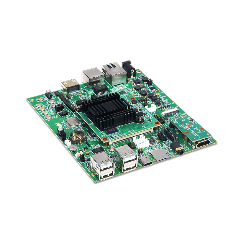
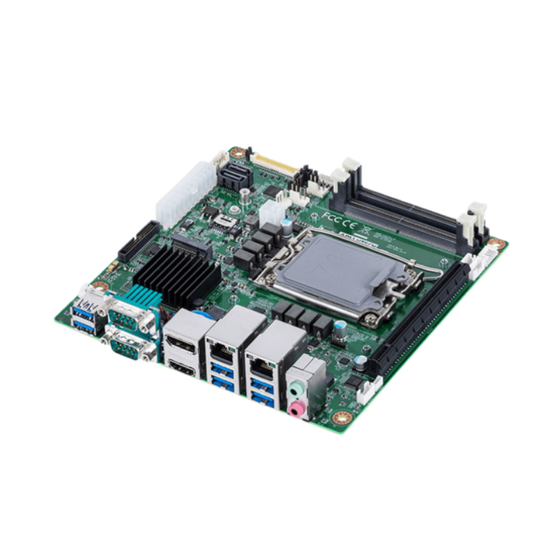
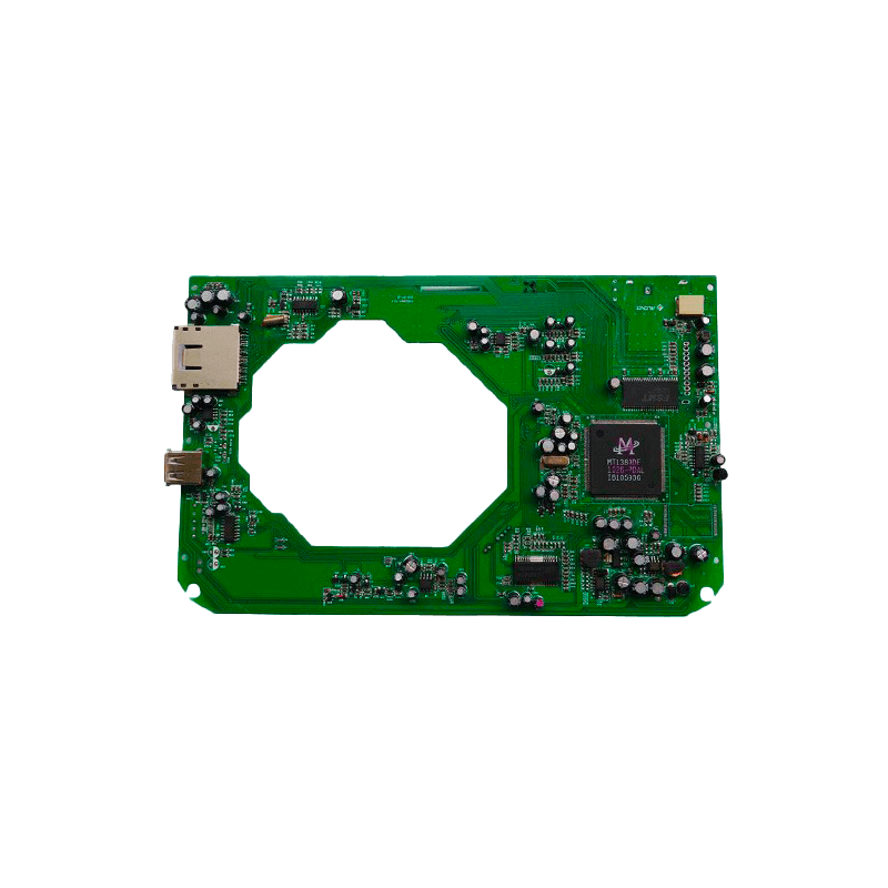
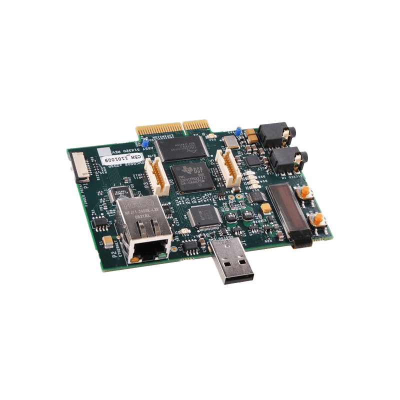
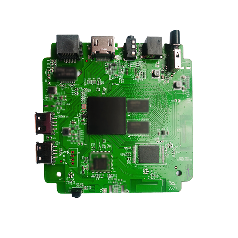
Communication PCB is a printed circuit board designed specifically for communication equipment, responsible for signal transmission, data processing, and hardware control functions. Its applications cover scenarios such as base stations, routers, optical modules, satellite communication, etc., and it needs to meet strict requirements such as high frequency, high speed, low loss, and high stability. As the hardware cornerstone of technologies such as 5G and the Internet of Things, communication PCBs directly affect communication speed and device reliability.
The main types of communication PCBs
PCB for base station
Used for 5G macro and micro base stations, mainly consisting of large-sized multilayer boards (12-30 layers), using high-frequency materials (such as Rogers 4350B), supporting millimeter wave frequency bands (above 24GHz), and the dielectric constant (Dk) needs to be stable within ± 0.05.
Fiber optic communication PCB
The core circuit board of the optical module needs to handle high-speed signals of 10Gbps or more, and low loss boards (such as M6G) are often used. The copper foil roughness is ≤ 2 μ m to reduce signal attenuation.
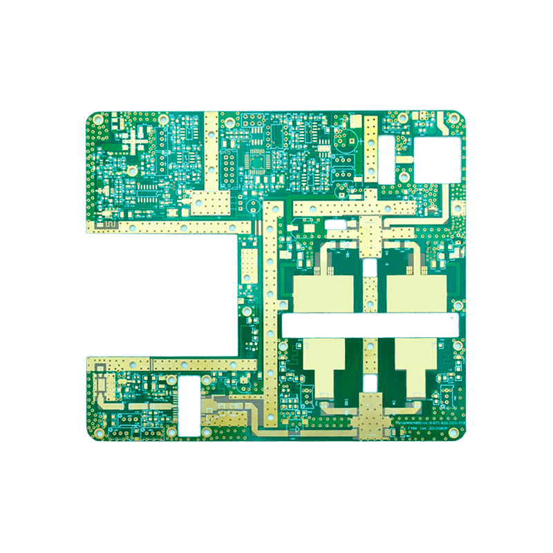
Microwave RF PCB
Satellite communication and radar equipment use PTFE substrate, which is resistant to high temperatures and has a dielectric loss (Df) of ≤ 0.002. It is equipped with buried resistance and capacitance technology to reduce external component interference.
Consumer grade communication PCB
Devices such as mobile phones and Wi Fi modules use HDI PCB (6-10 layers) with a line width/spacing of ≤ 50 μ m and blind hole aperture of ≤ 0.1mm to achieve high-density interconnection.
The core characteristics of communication PCB
High frequency signal processing capability
The working frequency of 5G base station PCB reaches 28GHz, requiring strict impedance control (± 5% error) and electromagnetic simulation optimization to reduce return loss.
High density and miniaturization
The PCB area of the mobile phone antenna module is less than 10cm ², integrating 10+RF traces, and using laser drilling and semi additive manufacturing (mSAP) to achieve micro hole processing.

Extreme environmental adaptability
The outdoor base station PCB needs to undergo temperature cycling testing between -40 ℃ and 125 ℃, with a surface coating of three proof paint, a protection level of IP67, and resistance to salt spray corrosion for over 500 hours.
Heat dissipation and power carrying capacity
The high-power RF unit adopts aluminum or copper substrate, with a thermal conductivity of ≥ 0W/m · K, and supports continuous power output of over 100W.
Why choose Syspcb
As a professional China manufacturer of communication PCBs,Syspcb specialize in the application of high-frequency materials and high-precision processing technology, and have provided PCBs for communication enterprises in more than 50 countries around the world. From 4G to 5G, from ground stations to the Internet of Things, we always focus on signal integrity, heat dissipation efficiency, and cost optimization to help build a more efficient global communication network. In the future, with the development of 6G and terahertz technology, we will continue to break through ultra-high frequency boards (Df ≤ 0.001) and 3D packaging processes, empowering the new era of intelligent connectivity for all things.