Table of Contents
What is HDI PCB?
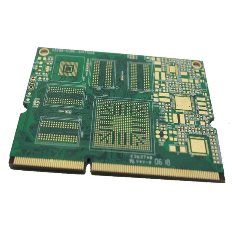
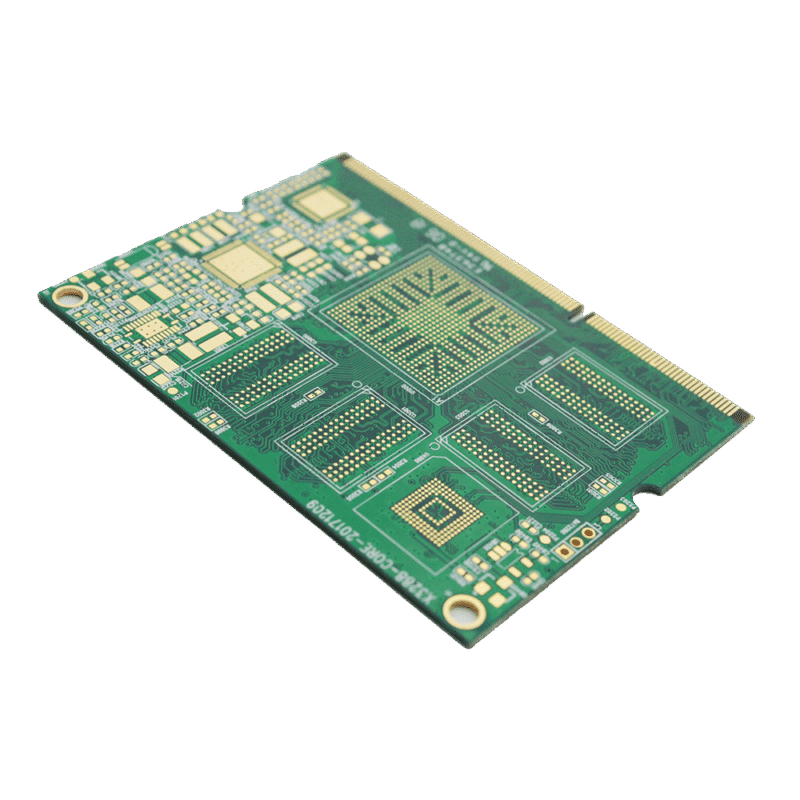
High density interconnects (HDI) PCB, represent one of the fastest-growing technologies in PCBs. Because of its higher circuitry density than traditional circuit boards, the HDI PCB design can incorporate smaller vias and capture pads, and higher connection pad densities. HDI Boards contain blind and buried vias and often contain micro vias of 0.006inch or less in diameter.
By using HDI technology, designers now can place more components on both sides of the raw PCB if desired. Now as the development of via in pad and blind via technology, it allows designers to place smaller components closer together. This means faster transmission of signals and a significant reduction in signal loss and crossing delays. HDI PCB is frequently found in mobile phones, touch-screen devices, laptop computers, digital cameras, 4G network communications, also prominently featured in medical devices.


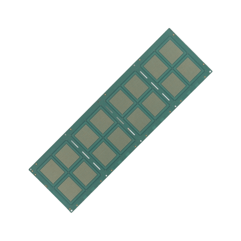
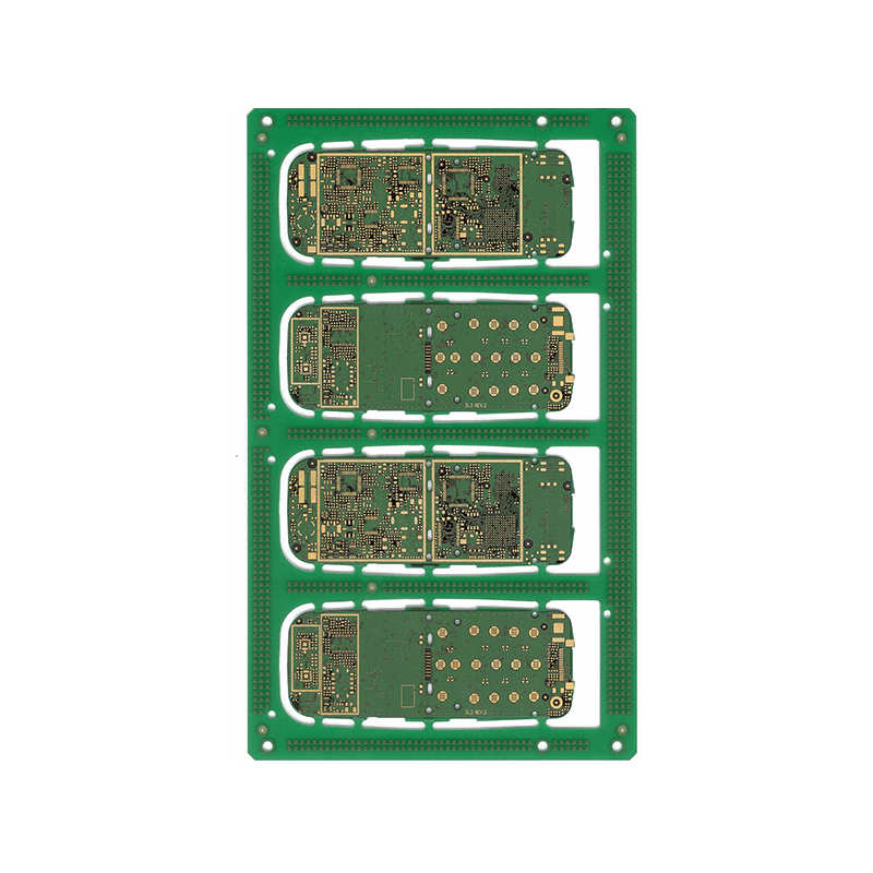
6 Layer HDI pcb microsection
Compare to standard Rigid PCB, HDI PCB request much higher wiring density with finer trace and spacing, smaller vias and higher connection pad density. Blind and buried vias’ design is one of their marked feature. HDI PCB are widely used for Cell Phone, tablet computer, digital camera, GPS, LCD module and other different area.
The advantages of HDI PCB include:
- Reduce the cost
- Better reliability
- Increase the wiring density
- Increase design efficiency
- Can improve the thermal properties
- In favor of the use of advanced packaging technology
- Has better electrical performance and signal correctness
- Can improve the radio frequency interference, electromagnetic interference and electrostatic discharge
Currently the advanced HDI technology we used include: “Copper Filled” for special stack microvia, “Laser Direct Imaging”(LDI) is specifically designed for fine line technology, to eliminate dimensional stability problem of artwork caused by environmental and material issues. “Direct Laser Drill”(DLD) is drilling of copper layer by direct CO2 laser irradiation, compare to additional laser drilling with conformal mask, the copper direct laser drilling is capable of providing higher accuracy, better hole quality and better efficiency for HDI projects
Four main differences between HDI PCB and traditional PCB
HDI (High-Density Interconnect) boards are compact circuit boards designed for small-capacity users. Compared to conventional PCBs, the most significant feature of HDI is its high wiring density. The differences between the two mainly focus on the following four aspects:
1. HDI is Smaller and Lighter
HDI boards are made by stacking multiple layers on a traditional double-sided core board. This method, known as Build-up Multilayer (BUM), involves continuous lamination. Compared to traditional circuit boards, HDI boards offer advantages such as being “light, thin, short, and small.”
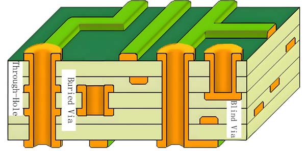
The electrical interconnection between layers in HDI boards is achieved through conductive vias, buried vias, and blind vias, which differ structurally from conventional multilayer PCBs. HDI boards use a large number of micro vias, and the drilling is done with lasers, whereas standard PCBs typically use mechanical drilling, leading to a reduced layer count and aspect ratio.


2. HDI Mainboard Manufacturing Process
The high density of HDI boards is primarily reflected in the vias, traces, pad density, and inter-layer thickness.
- Micro Vias: HDI boards contain blind vias and micro vias, with hole diameters less than 150um. This requires advanced technology for hole formation, as well as tight control over cost, production efficiency, and hole position accuracy. Conventional multilayer PCBs do not have micro vias like HDI boards.
- Fine Trace Width and Spacing: HDI boards require stricter standards for trace defects and surface roughness. Generally, trace width and spacing do not exceed 76.2um.
- High Pad Density: The pad density for solder joints exceeds 50 per square centimeter.
- Thinner Dielectric Layers: The trend for HDI boards is to reduce inter-layer dielectric thickness to 80um or less, with increasingly stringent requirements for uniformity, especially for high-density boards and package substrates with controlled impedance.
3. Better Electrical Performance of HDI Boards
HDI not only enables smaller product designs but also meets higher standards for electronic performance and efficiency.
The increased interconnect density in HDI boards allows for enhanced signal strength and improved reliability. Additionally, HDI boards offer better performance in terms of radio frequency interference, electromagnetic interference, electrostatic discharge, and heat conduction. HDI also uses digital signal processing (DSP) technology and several patented technologies, providing full-load adaptability and strong short-term overload capacity.
4. HDI Boards Have Strict Requirements for Buried Vias and Plugging
As seen above, HDI boards outperform conventional PCBs in terms of both size and electrical performance. However, HDI manufacturing involves more challenges due to its higher production thresholds and complexity—particularly in terms of buried via plugging.
The main production pain points and difficulties in HDI manufacturing involve the plugging of buried vias. If the buried via plugging is not done properly, significant quality issues may arise, such as uneven board edges, irregular dielectric thickness, and uneven pads.
- Uneven Board Surface: The board may exhibit surface irregularities, leading to “beach” phenomena that can cause trace breaks, line interruptions, and other defects.
- Impedance Variations: Variations in dielectric thickness can lead to unstable signal transmission due to fluctuating characteristic impedance.
- Uneven Pads: Uneven pads can lead to poor subsequent packaging quality, resulting in component failure or damage.
General Specification for HDI PCB
Layer Count: 4-20Layers
Type of stack up: 1+N+1, 2+N+2
Stand Process Flow for 1+4+1
Material Available: FR4, High Tg FR4, Halogen Free FR4
Board thickness: 0.4-3.2mm
Finished copper thickness: 1/3oz – 3oz
Min trace width/spacing: 3/3mil
Min through hole: 0.2mm
Min blind via: 0.1mm
Surface treatment: Immersion Gold, ENIG + OSP
SysPCB: An Experienced Chinese HDI PCB Supplier
SysPCB is one of the best HDI PCB suppliers in China, with over 10 years of professional production experience and expertise in manufacturing HDI printed circuit boards. You can rest assured to choose us as your partner, as we have the following advantages:
No MOQ
SysPCB does not have a minimum order quantity (MOQ) requirement, so you can confidently partner with us. As an HDI PCB manufacturer, we are committed to building long-term relationships based on mutual trust and benefit.
One-Stop Service
If you’d like to avoid the hassle and skip some steps, you can opt for our one-stop turnkey service. SysPCB can manage the entire process for you, with clear and transparent workflows that help save you time and effort. Once the order is placed, all you need to do is wait for the delivery of your goods.
Comprehensive Pre-Sales and After-Sales Support
SysPCB offers dedicated pre-sales support with a professional customer service and technical team available to assist with any inquiries or consultations at your convenience. Post-sales, we are committed to addressing any quality issues by offering rework services or appropriate compensation. Ensuring a positive customer experience is a core value of our company, and we strive to provide exceptional service at every stage of your engagement with us.