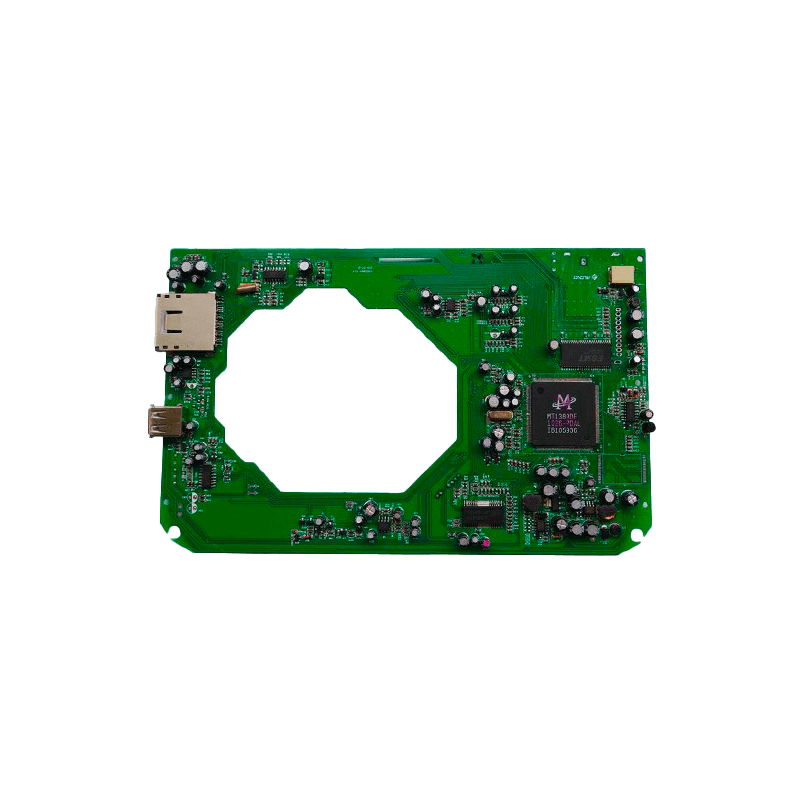
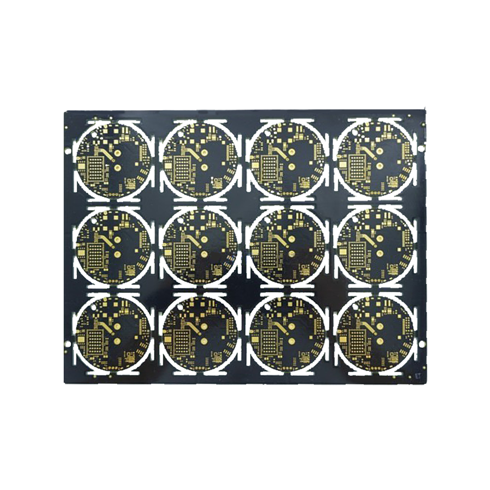
As a professional manufacturer of medical PCBs, we specialize in the field of high reliability circuit boards and focus on providing core electronic support for monitors, imaging equipment, implantable devices, and more. Medical equipment is directly related to the safety of patients’ lives, and PCBs need to meet the requirements of extreme environmental stability, long-term durability, and biocompatibility. Industry data shows that the global medical PCB market is expected to exceed $3.2 billion by 2026, with high precision, miniaturization, and anti-interference capabilities becoming key competitive factors.
Table of Contents
Medical PCB and its Benefits
Material compliance
The substrate must be free from harmful substances such as lead and halogens. Implantable device PCBs often use polyimide (PI) substrates, which are resistant to high temperatures and corrosive to antibody solutions.
Accuracy control
Medical equipment tends towards miniaturization, with a line width/spacing of ≤ 75 μ m and an aperture of ≤ 0.15mm. Laser drilling and LDI (Laser Direct Imaging) technology can ensure micrometer level machining accuracy.

reliability verification
Must pass 85 ℃/85% humidity aging test, 500 or more temperature cycles (-40 ℃~125 ℃), and EMC anti-interference test, with a failure rate of less than 0.01%.
cleaner production
The workshop needs to meet the Class 10000 dust-free standard to avoid dust pollution. Vacuum reflow soldering is preferred as the welding process to reduce the risk of oxidation.
Limitations of medical PCB
Strict certification cycle
A medical PCB needs to pass multiple certifications such as FDA, CE, GMP from research and development to mass production, with a lead time of 12-24 months, far exceeding the 3-6 month standard for consumer electronics.
The contradiction between miniaturization and heat dissipation
Implantable devices require PCB size<10mm ², but high integration can easily lead to local overheating. Traditional heat dissipation designs are difficult to be compatible and require innovative solutions such as buried copper blocks or ceramic substrates.


Long life cycle management
The service life of medical equipment often exceeds 10 years, and PCB suppliers need to retain raw material formulas and process files for at least 15 years, placing extremely high demands on supply chain stability.
Low cost sensitivity but lower fault tolerance
The price of medical PCBs can reach 3-5 times that of similar consumer electronics products, but any minor defects may trigger recall risks. Manufacturers need to invest over 30% of additional costs in the quality control process.
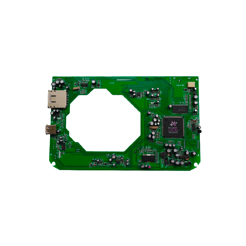
Types of Medical PCB
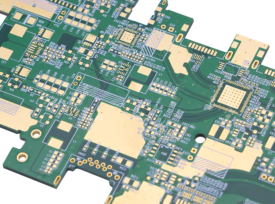
HDI and Class Carrier Board Technology
Used for high-frequency scenarios such as CT machine control modules, HDI PCB with more than 10 layers can reduce signal delay, and impedance control accuracy needs to reach ± 5%.
Flexible Circuit Board (FPC)
Suitable for flexible devices such as endoscopes, with a bending radius of less than 3mm, and gold plating process to enhance interface durability.
Rigid Flex PCB
Rigid Flex PCB:Implementing 3D wiring in pacemakers reduces connector usage and lowers system failure rates by 40%.
Application areas of medical PCB
Medical PCB (printed circuit board), as the core component of medical electronic devices, is applied throughout the entire process of diagnosis, treatment, monitoring, and health management, mainly covering the following areas:
Life monitoring equipment
Application scenarios: Real time monitoring devices such as electrocardiogram monitors, ventilators, and oximeters.
Technical requirements: High stability PCB is required, supporting weak signal acquisition (such as μ V level electrocardiogram signals), using 4-6 layers of multi-layer boards, with anti electromagnetic interference design.
Medical imaging diagnostic equipment
Application scenarios: CT、MRI、 High end imaging systems such as ultrasound diagnostic equipment and X-ray machines.
Technical requirements: High frequency and high-speed signal processing, using 8-12 layer HDI board or high-frequency board (such as Rogers RO3000 series), with impedance control accuracy of ± 3%.

In vitro diagnostic (IVD) equipment
Application scenarios: Biochemical analyzers, PCR machines, blood glucose meters and other detection equipment.
Technical requirements: High precision temperature control and signal amplification circuit, commonly used thick copper PCB (copper thickness ≥ 3oz) to enhance current load capacity, and adopt three proof coating for corrosion prevention.
Surgical and therapeutic equipment
Application scenarios: endoscopes, laser surgical knives, electrocauters, dialysis machines, etc.
Technical requirements: High voltage resistant design (>1000V), using ceramic substrate or high TG material (Tg ≥ 170 ℃), some equipment needs to be waterproof (IP67 level).
Why choose SysPCB
Medical PCB manufacturing is a dual test of technology and responsibility. We have obtained ISO 9001:2015 medical system certification and established a full chain control system from material selection to failure analysis, providing over 50 million zero defect PCBs to more than 200 medical enterprises worldwide.
At SYS Technology, we are responsible for manufacturing of PCB and assembly of medical PCBA, so you can spend more time running your business in marketing of medical devices. Even if you only need to assemble a small amount of equipment, we can quickly and accurately meet your needs. To learn more about how SYS Technology can help you, contact us today!