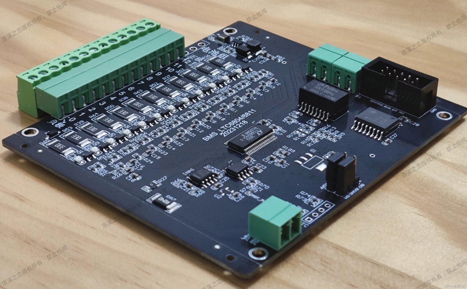
In the battery management system (BMS), the core safety barrier of new energy vehicles, the protection board is like the “nerve center” of the battery pack, and its reliability directly determines the overall safety of the vehicle. In the manufacturing of BMS protection boards, the crimping process is reshaping the standard of PCB connection reliability with revolutionary solder free technology.
Table of Contents
1、 Press-Fit: technological breakthrough in battery protection board connection
The connection between FFC/FPC (flexible cable/circuit board) and PCB in traditional battery protection boards relies on welding, which requires the addition of reinforcement boards, intermediate connectors, and other components. The process is complex and there is a risk of welding detachment. The crimping process achieves a fundamental change through two disruptive operations:
1. Puncture crimping: Use a high-precision crimping machine to pierce the FFC/FPC insulation layer through the terminal, directly forming a mechanical electrical integrated connection with the conductor without the need for solder.
2. Modular plug-in: Insert the crimped terminals into the female connector, and then connect the PCB board end connector as a whole, shortening the assembly process by more than 40%.
Taking TE Connectivity’s NanoMQS solution as an example, its crimping terminals adopt an “eye shaped hole” elastic structure, which produces interference fit after being pressed into PCB through holes. The ability to withstand vibration and impact is 50% higher than that of soldering, completely avoiding material thermal stress degradation caused by high temperature soldering.
2、 Why has crimping technology become an inevitable choice for BMS PCB?
1. Dual improvement of safety and reliability
The battery pack is exposed to a high temperature environment of 80-90 ℃ for a long time, and the welding points are prone to microcracks due to thermal fatigue, resulting in increased impedance or even circuit breakage. The non thermal characteristics of the crimping process avoid thermal stress damage, and the stable connection resistance is below 0.5m Ω, ensuring accurate transmission of cell sampling signals.
2. Breakthrough in the intensification of space and cost
-Space saving: The crimping solution eliminates the need for reinforcement plates, transition connectors, and other components required for traditional welding, reducing the thickness of the connection structure by 60% and adapting to the layout requirements of “every inch of land and every inch of gold” in battery packs.
-Cost optimization: Material costs are reduced by 30% (eliminating solder and flux), and assembly efficiency is significantly improved, eliminating the need for wave soldering/reflow soldering equipment and shortening production cycles.
3. The essential need to adapt to high vibration environments
New energy vehicles continue to face vibration impacts during operation. The mechanical anchoring effect of the crimping point can withstand a vibration acceleration of 20G, much higher than the 5G upper limit of the welding point, significantly reducing the risk of battery sampling line failure.
3、 The core requirements of crimping process for PCB design and manufacturing
To fully leverage the advantages of crimping, the battery protection board PCB needs to meet strict process adaptation conditions:
▶ Selection of high-temperature resistant substrate
Using PTFE (polytetrafluoroethylene) semi cured board as the core material, with a glass transition temperature (Tg) greater than 280 ℃, to ensure the stability of the PCB laminated structure in the high-temperature environment of the battery pack.
▶ High precision control of through-hole technology
-Aperture tolerance: The gap between the crimping pin and PTH (plated through-hole) should be controlled within ± 0.05mm. Insufficient interference can cause loose connections, while excessive interference can cause tearing of the hole wall.
-Hole wall quality: roughness ≤ 20 μ m, copper thickness ≥ 25 μ m. The adhesive residue is removed and the copper adhesion is enhanced through plasma activation process (nitrogen hydrogen mixed gas).
▶ High voltage protection design
The leakage voltage of the battery module can reach 3000V, and it is necessary to use high-voltage anti welding ink (such as PSR-2000 ME8-160PS) and adopt the “character screen printing first and then anti welding” process to prevent the label from falling off.
4、 Collaborative process: integration and application of crimping and peripheral technologies
The crimping process needs to be coordinated with other key processes to build a complete high reliability battery protection board manufacturing system:
-Spot welding reinforcement: The connection between the protective plate and the battery nickel strip adopts double pulse spot welding, with a welding point tension of>2.0kgf and no burrs or blackening after welding.
-Bottom filling adhesive protection: Apply modified epoxy resin filling adhesive to BGA chips to enhance their drop resistance (tested through a 1.5m drop test). The curing temperature should be ≤ 110 ℃ to avoid damaging the crimping points.
-Fixture adaptation for tinning: When the plug-in is passed through the soldering furnace, a hollow fixture is used to isolate the crimped area, exposing only the plug-in solder pads to prevent secondary heating of the crimped terminals.
5、 Future trend: Intelligent upgrade of crimping process
With the improvement of battery pack energy density and the integration of BMS functions, the crimping process is evolving in two dimensions:
1. Micro spacing crimping: The terminal spacing has been reduced from 1.0mm to 0.4mm, supporting higher density battery sampling signal transmission;
2. Online monitoring: The force displacement curve monitoring technology determines the quality of crimping in real time, and the defect rate approaches 0.
>Industry consensus: By 2025, the penetration rate of crimping technology in the global new energy vehicle battery protection board PCB market will exceed 60%, becoming a “standard” technology for highly reliable BMS.
Conclusion: Anchoring Safety Boundaries with Technological Innovation
The crimping process provides a “zero thermal stress” connection solution for new energy vehicle battery protection boards through its three major advantages of no welding, anti vibration, and space saving. For PCB companies, mastering key technologies such as PTFE substrate processing, plasma activated hole walls, and micrometer level through-hole control will become the core chips in competing for the high-end BMS market. In this wave of energy revolution, only by incorporating technological innovation into every inch of the circuit can we uphold the safety commitment of putting life first.
>The connection is like breaking a cow in a pot, the balance between force and softness is a precise stitching without shadows. “- A note by an automotive electronics engineer