Table of Contents
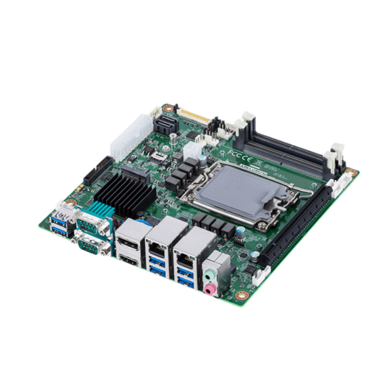
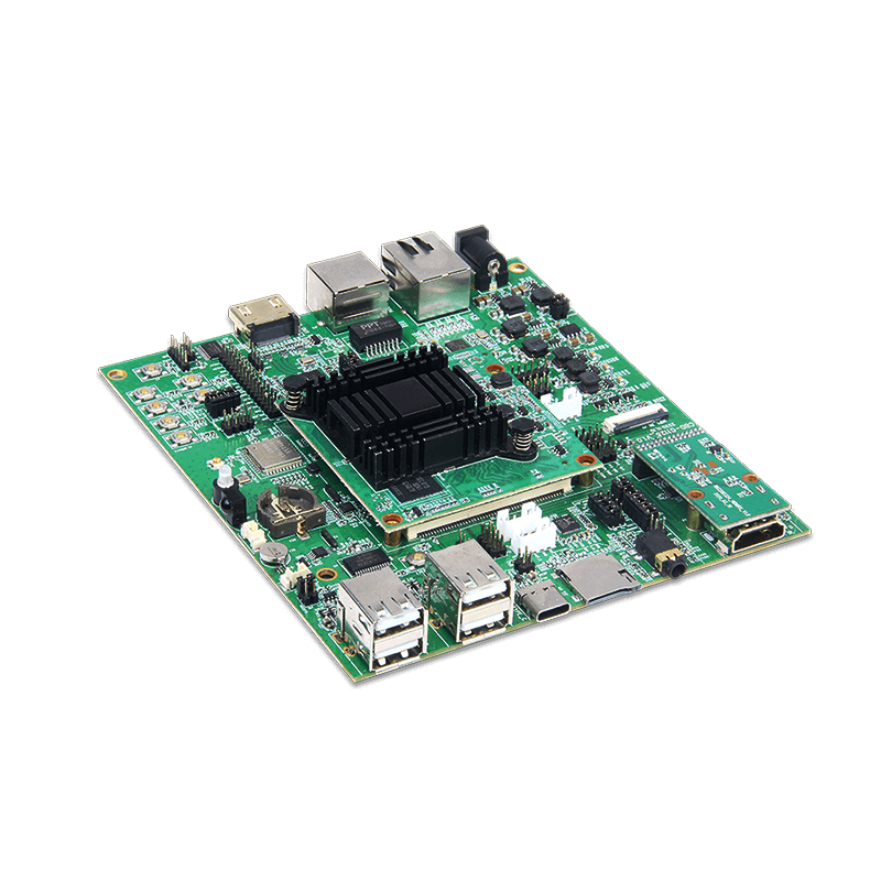
What is an IoT PCB(Internet of Things PCB)?
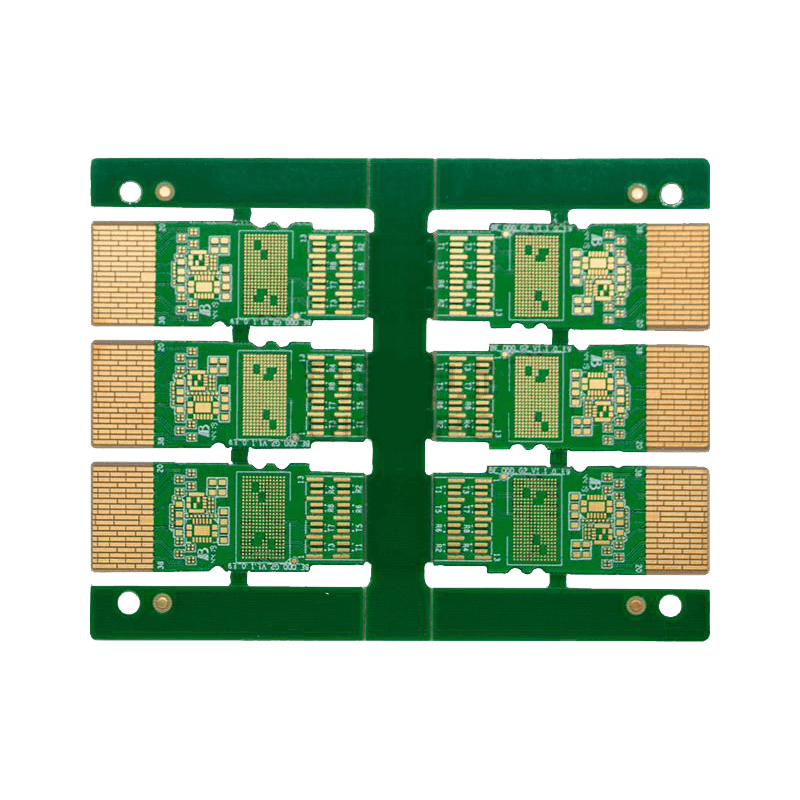
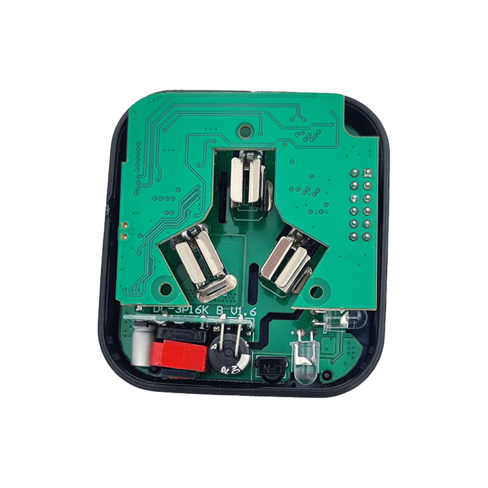
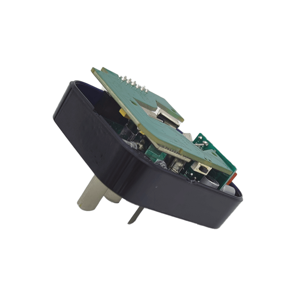
The IOT PCB is a printed circuit board specially designed for intelligent interconnection devices, which undertakes the functions of sensor data acquisition, wireless communication and edge computing. Its core features include low power consumption, high integration, and strong environmental adaptability, supporting multiple communication protocols. As the “nerve center” of IoT terminals, their performance directly determines the device’s response speed, energy efficiency ratio, and long-term stability.
Application areas of IoT PCB
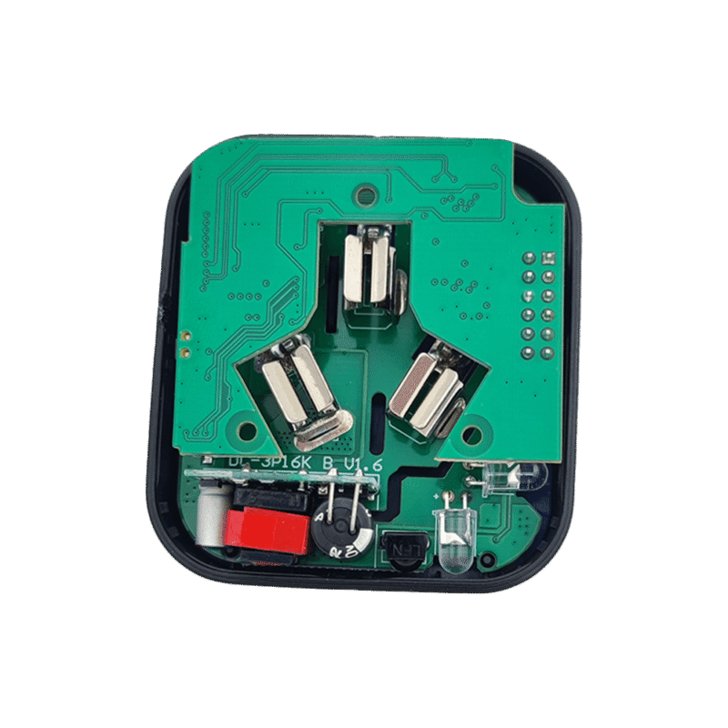
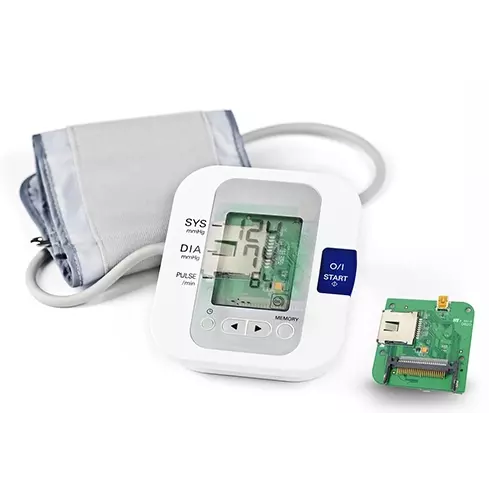
Smart Home
Temperature controllers, smart door locks, and other devices use 2-4 layer PCB and integrate Wi Fi/Bluetooth dual-mode communication. The standby power consumption is less than 10 μ A, and the signal coverage radius can reach 50 meters.
Industrial Internet of Things (IIoT)
Factory sensors and PLC controllers require 6-8 layers of anti-interference PCBs, supporting RS-485/Modbus protocol, operating at temperatures ranging from -40 ℃ to 85 ℃, and sensor PCBs with a lifespan of over 100000 hours.
Smart Agriculture
Soil monitoring instruments and irrigation controllers require a three proof coating PCB (IP67 protection), with a humidity resistance of 100% RH, and a drone PCB that can withstand pesticide corrosion for over 5000 hours.
What factors need to be considered in the design process of IoT PCB
The design of IoT PCB needs to consider multiple factors comprehensively to ensure its stable and efficient operation in IoT devices. The following are the key factors that need to be considered during the design process:

Functional requirements
Clarify the specific functions of IoT devices, such as data acquisition, processing, transmission, etc. Determine the required electronic components such as chips, sensors, communication modules, etc. based on the functions, and plan the layout space on the PCB reasonably to ensure smooth electrical connections and signal transmission between each component.
Signal integrity
There are various signals in IoT devices, such as analog signals, digital signals, high-frequency signals, etc. To ensure accurate signal transmission, it is necessary to design wiring reasonably to reduce signal reflection, crosstalk, and attenuation. For example, separating high-speed signal lines from low-speed signal lines and implementing shielding measures for sensitive signals.
Power management
Design efficient and stable power circuits to meet the voltage and current requirements of different components. At the same time, considering the anti-interference ability and power efficiency of the power supply, in order to reduce energy consumption and extend the battery life of battery powered equipment. If a power filter is used to remove high-frequency noise from the power supply and a suitable power chip is selected to achieve efficient voltage conversion.
Electromagnetic compatibility
IoT devices are usually located in complex electromagnetic environments. Reasonable PCB layout, shielding design, and filtering measures should be taken to reduce electromagnetic interference between internal components of the device and between the device and the external environment, ensuring that the device can work normally in various electromagnetic environments.

Reliability
IoT devices may require long-term operation, so PCB design should consider reliability. Choose reliable electronic components and PCB materials, adopt reasonable soldering processes and packaging forms, improve the mechanical strength and stability of PCBs to adapt to different working environments, such as temperature, humidity, vibration, and other changes.
Size and space limitations
Based on the external dimensions and internal spatial structure of IoT devices, design the size and shape of PCBs reasonably, optimize component layout, and minimize the size of PCBs as much as possible while meeting functional requirements to meet the design requirements of miniaturized and portable devices.
Cost control
On the basis of meeting design requirements, try to choose cost-effective electronic components and PCB materials, optimize design schemes, reduce unnecessary processes and cost expenditures, in order to reduce product costs and improve market competitiveness.
Security
For some IoT devices that involve personal safety or important data, the security of PCB design should be considered. For example, using isolation circuits to prevent electrical accidents, designing encryption circuits to protect data security, etc.
Why choose Syspcb?
As a professional China manufacturer of IoT PCBs, we have served IoT enterprises in 50 countries worldwide and delivered over a million highly reliable PCBs. By independently developing low dielectric loss materials and ultra precision laser drilling technology, the product yield has exceeded 99.2%. In the future, with the integration of AIoT and 6G technologies, we will provide more efficient and green hardware solutions for the intelligent connection of all things.