Table of Contents
What is a communication PCB?
Communication PCB is a printed circuit board designed specifically for information transmission, responsible for RF signal processing, data exchange, and wireless connection functions. In the field of consumer electronics, it is widely used in devices such as mobile phones, routers, and smart homes, serving as a hardware carrier for communication technologies such as Wi Fi, Bluetooth, and 5G. Its performance directly affects network speed, signal stability, and device endurance.
Consumer Electronics PCB Main application areas
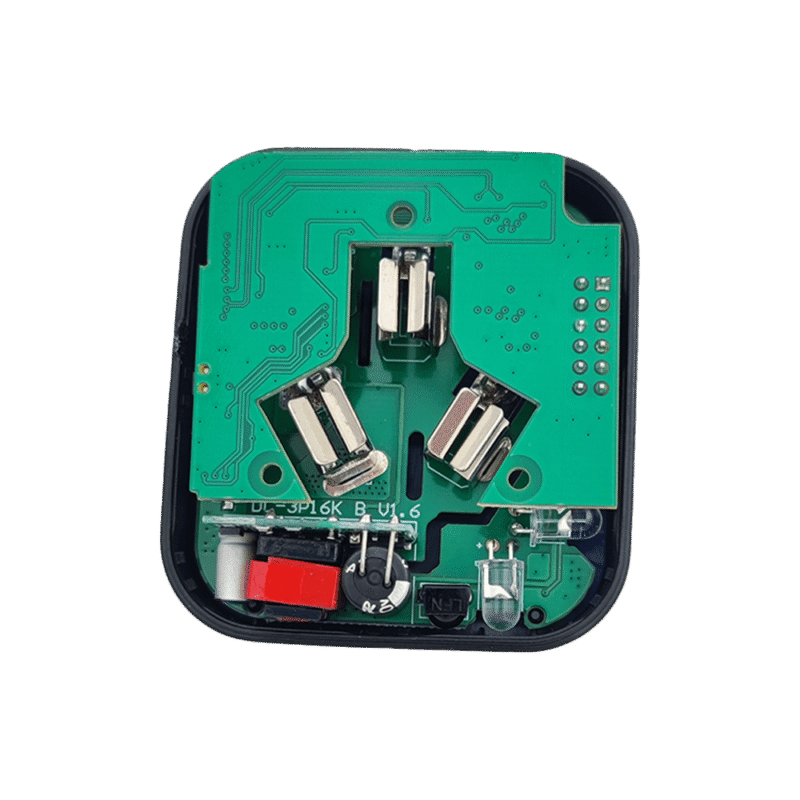
Wireless IoT devices
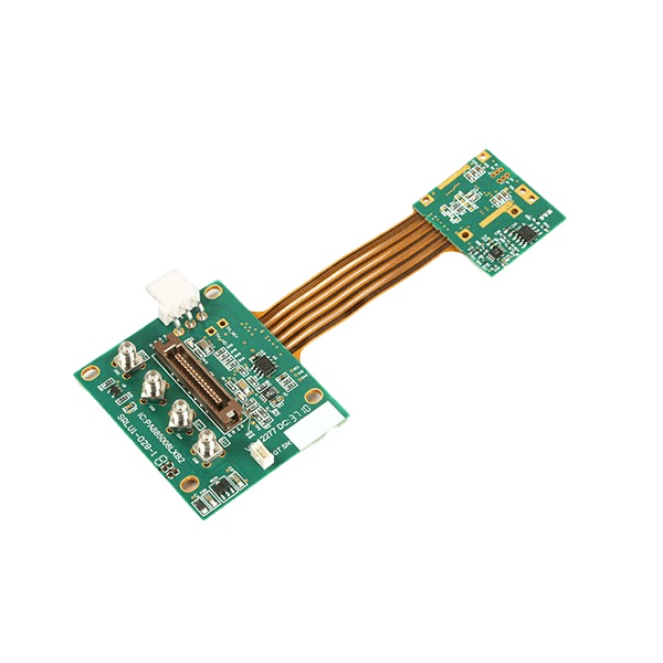
Smart watches and smart speakers rely on Bluetooth/Wi Fi module PCBs with an area of less than 5cm ², using flexible circuit boards (FPCs) to adapt to curved designs, and a PCB bending life of over 100000 times.
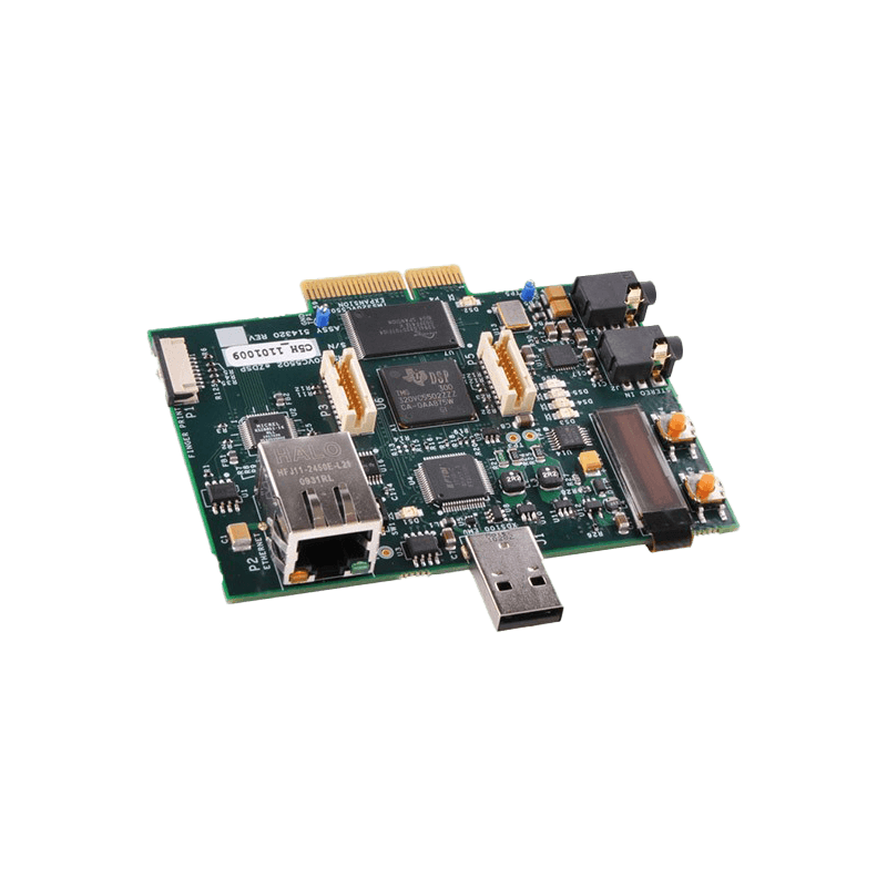
Network terminal equipment
Routers and optical modems require high-speed signal processing and use low loss boards (such as FR-4 high-frequency version) to support 10Gbps Ethernet transmission
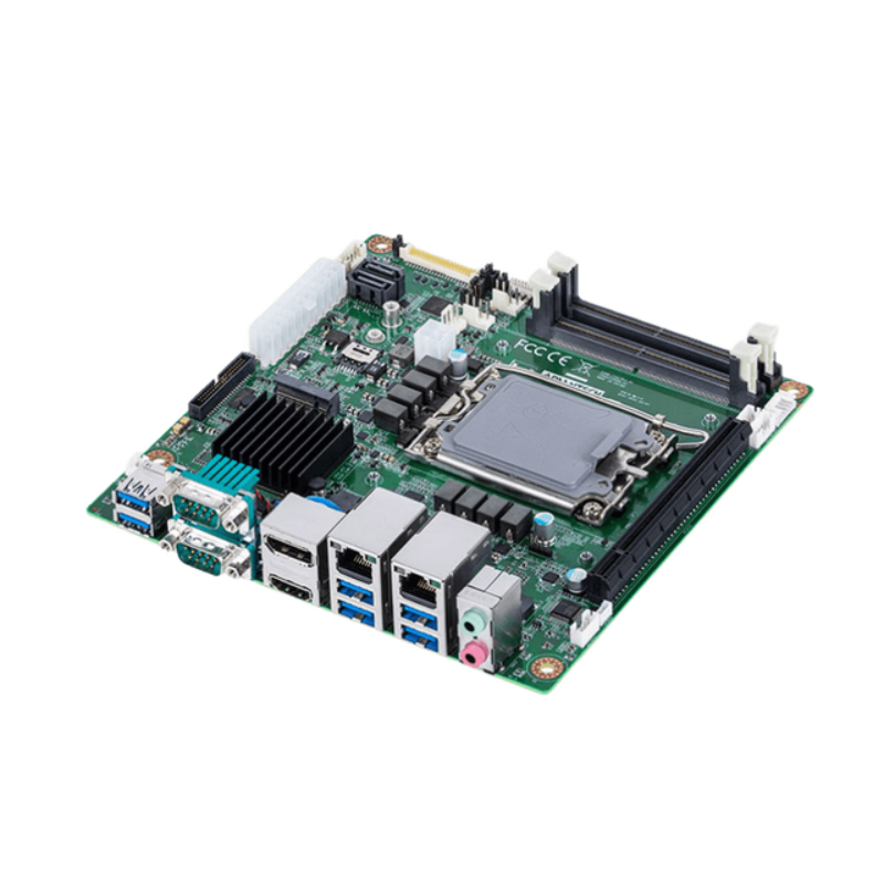
Vehicle mounted intelligent terminal
The car networking module adopts a high-temperature resistant PCB (Tg ≥ 170 ℃), which has passed environmental testing at -40 ℃~105 ℃. The PCB of the car entertainment system can integrate 4G/5G dual-mode communication.
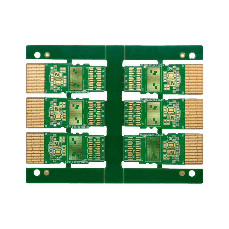
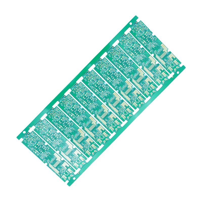
The main types of communication PCBs

High frequency high-speed board
Used for 5G mobile phones and base stations, the material is mainly Rogers RO4350B, with a dielectric constant (Dk) of 3.48 ± 0.05, and signal loss is reduced by 60% compared to ordinary FR-4.
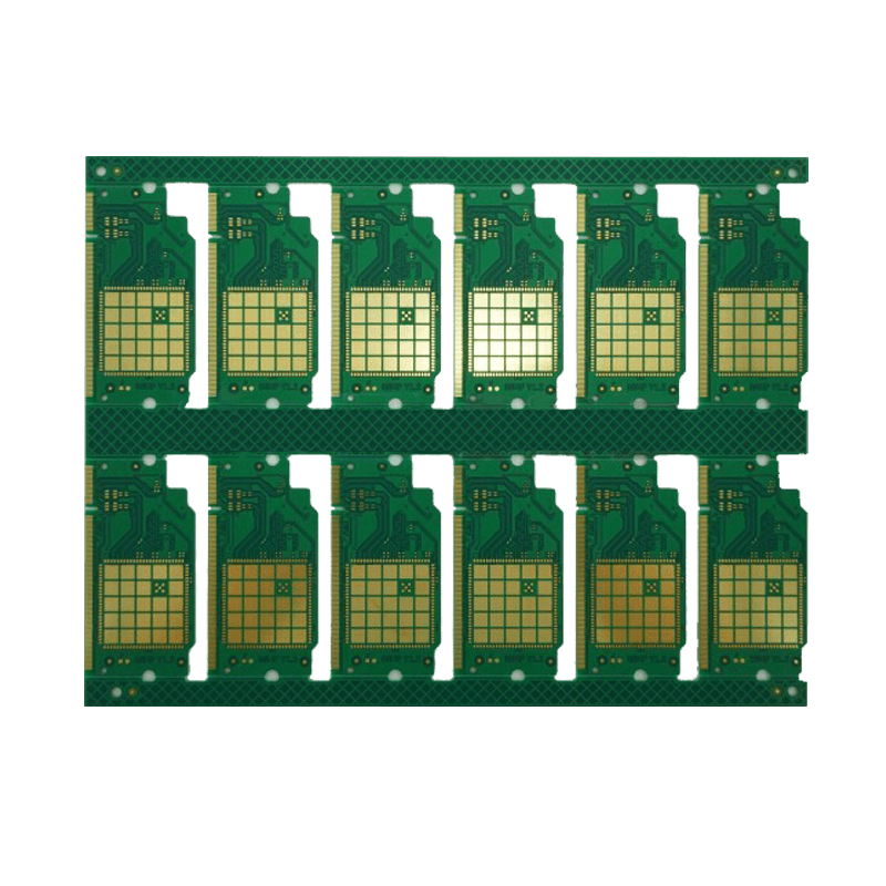
HDI high-density board
The mobile phone motherboard adopts 8-12 layers of any layer interconnect (Any layer HDI), with a line width/spacing of ≤ 40 μ m and a blind hole aperture of 0.1mm
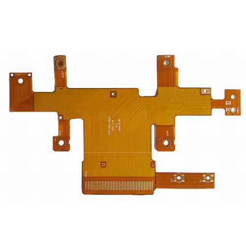
Flexible Circuit Board (FPC)
Flexible wiring is implemented in wearable devices with a bending radius of less than 3mm. OPPO wristbands use two-layer FPC with a thickness of only 0.1mm.
Metal substrate
The high-power router cooling module uses an aluminum substrate with a thermal conductivity of ≥ 2.0W/m · K, and the router PCB can carry a continuous power of 30W.
The core characteristics of communication PCB
Low loss and high stability
5G RF PCB insertion loss<0.3dB/inch, impedance control accuracy ± 5%, operating temperature range -40 ℃~125 ℃.
Anti interference design
By using ground hole shielding and differential routing technology, the signal-to-noise ratio of the Wi Fi 6E device PCB has been improved by 40%, and the delay has been reduced to 2ms.
Environmental protection and durability
Compliant with RoHS standards, lead-free soldering process, and mobile phone PCB all require 1000 hours of salt spray testing.
Why choose SysPCB?
We prioritize our customers, offering exceptional support and prompt responses to inquiries at any time. Here’s why SysPCB is the ideal choice for your Consumer Electronics PCB needs:
- Extensive Expertise: Over a decade of experience in Consumer Electronics PCB manufacturing.
- Affordable Solutions: Competitive pricing with no minimum order quantity (MOQ) and flexible, negotiable terms.
- Superior Quality: High-quality assurance backed by professional production facilities.
- Comprehensive Services: End-to-end solutions with a strong focus on customer satisfaction throughout the process.
- Timely Delivery: Fast turnaround times paired with reliable post-sales support.