Table of Contents
Executive Summary
The rapid deployment of 5G networks and the exponential growth of data centers have positioned optical modules as critical components in modern communication infrastructure. These modules, which perform essential electro-optical conversion, rely on specialized printed circuit boards (PCBs) capable of handling high-frequency signals with minimal loss. For PCB manufacturers, understanding the unique requirements of 5G optical module PCBs—including signal integrity, thermal management, and impedance control—is crucial for delivering reliable, high-performance solutions. This comprehensive guide explores the key technologies, materials, and manufacturing processes that enable PCBs to meet the demanding specifications of 100G, 400G, and emerging 800G/1.6T optical modules, while highlighting industry trends and standardization efforts shaping this rapidly evolving market.
1.Introduction to 5G Optical Modules and PCB Requirements
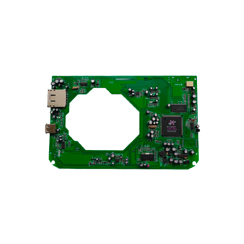
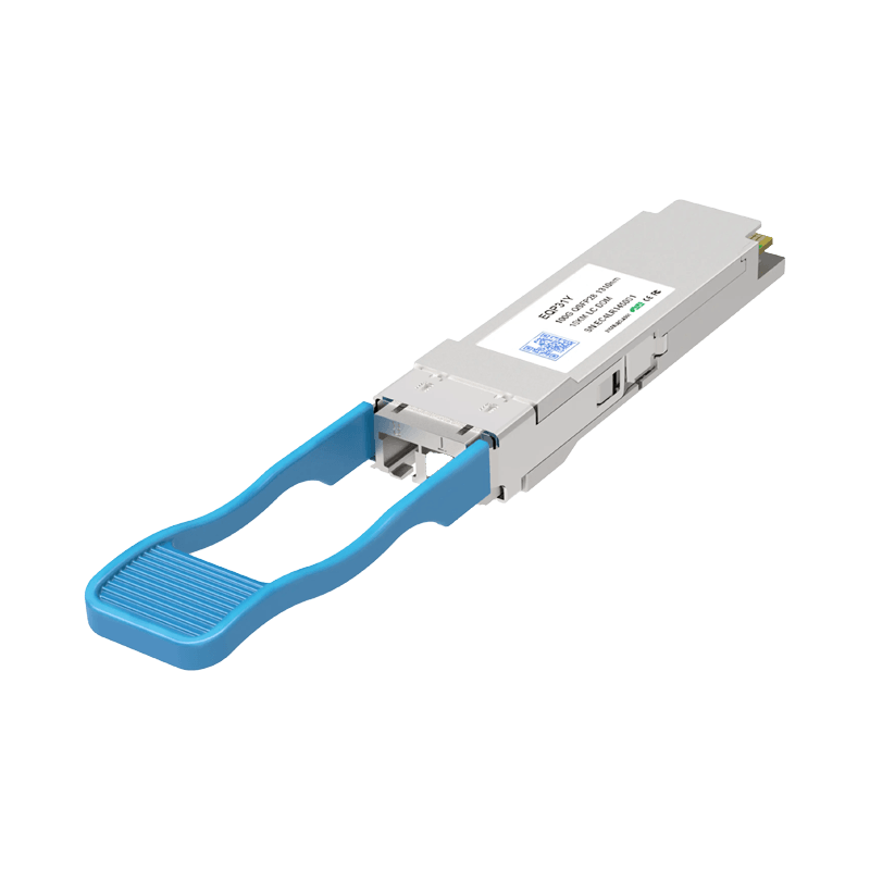
5G optical modules are essential components that facilitate the conversion between electrical signals and optical signals in 5G networks and data center applications . These modules enable high-speed data transmission across various communication infrastructure, including telecom carrier networks, access networks, data centers, and Ethernet systems . As 5G technology introduces broader bandwidths and lower latency applications, the carrier network architecture requirements have significantly evolved, making optical modules with advanced PCBs indispensable for modern communication systems.
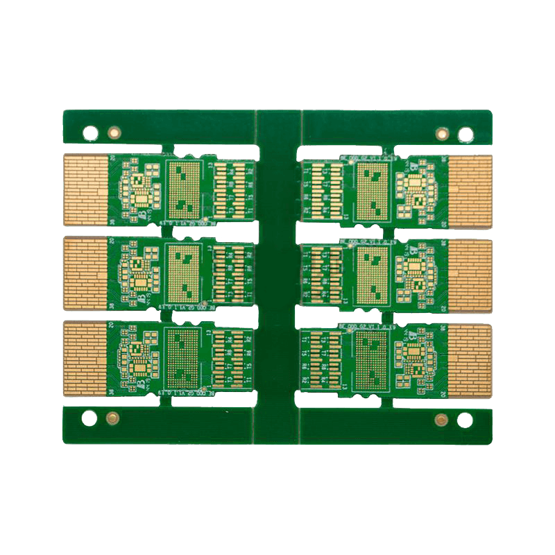
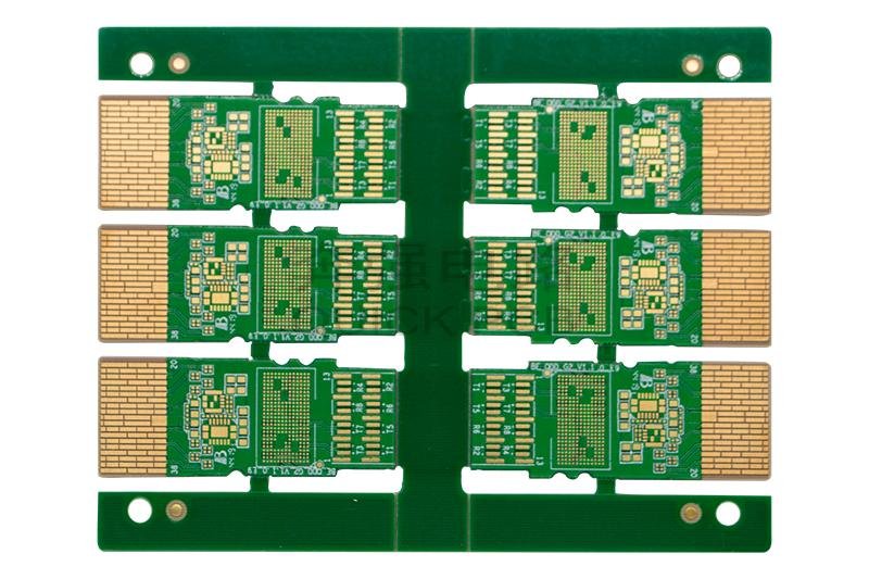
The PCBs for optical modules serve as the fundamental platform for mounting and interconnecting various components, including optical subassemblies, driver chips, and control circuitry. Unlike standard PCBs, optical module PCBs must address several unique challenges:
– Maintaining signal integrity at high frequencies (up to 50 GHz and beyond)
– Managing heat dissipation from high-power components
– Ensuring precise impedance control for high-speed differential pairs
– Providing stable dielectric properties across varying environmental conditions
With data rates advancing from 100G to 400G, 800G, and eventually 1.6T, the demands on optical module PCBs continue to intensify, requiring specialized materials, sophisticated design techniques, and precision manufacturing processes to meet stringent performance requirements .
2.Key Technical Requirements for 5G Optical Module PCB
2.1 Signal Integrity and Low-Loss Transmission
Maintaining signal integrity is paramount for optical module PCBs operating at 5G frequencies. As data rates increase to 400G and beyond, even minor imperfections in the PCB can cause significant signal degradation . Key considerations include:
•Controlled Impedance: Tight impedance tolerances of ±5% or better are essential for high-speed differential pairs to minimize signal reflections and ensure proper impedance matching .
•Minimized Insertion Loss: PCBs must exhibit low dielectric and conductor losses at high frequencies. This requires materials with low dissipation factors (Df) and smooth copper foils to reduce surface roughness effects .
•Crosstalk Mitigation: Proper spacing, grounding, and shielding techniques are necessary to prevent electromagnetic interference between adjacent high-speed channels.
Advanced design strategies such as multi-channel signal transmission line parallel design and careful stack-up planning help maintain signal integrity across the entire PCB .
2.2 Thermal Management Solutions
Thermal management represents a critical challenge in 5G optical module PCBs due to the significant heat generated by high-power optical components and processing chips. Effective thermal management strategies include:
•Thermal Via Arrays: Implementing patterns of thermal vias under heat-generating components to transfer heat to inner ground planes or dedicated thermal layers.
•Specialized Heat Dissipation Structures: Innovative approaches such as Foil-pressed embedded copper blocks create efficient thermal pathways while maintaining electrical performance .
•Component Embedding: Techniques like laser-direct machining of step slots on copper blocks allow for component下沉 (sinking) to any specified layer, improving both thermal performance and spatial efficiency .
•Thermal Interface Materials: Using specialized materials such as tri-composite aluminum sheets as buffer materials during copper block embedding processes, matched to the dynamic viscosity curve of the lamination program to ensure buffer effects while avoiding molding issues .
Proper thermal management not only ensures reliable operation but also extends the lifespan of optical modules by preventing thermal stress-related failures.
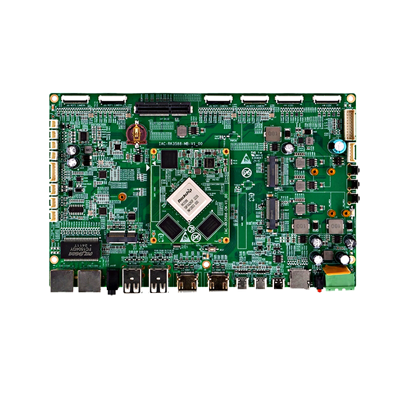
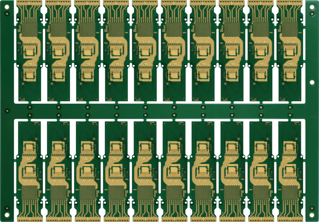
2.3 High-Density Interconnect (HDI) Technology
The miniaturization trend in optical modules demands increasingly dense PCB designs with finer features and more complex interconnect schemes. High-Density Interconnect (HDI) technology addresses this need through:
•Fine Line Fabrication: Achieving trace widths and spaces of 3.0mil/3.0mil (line width/space) or less for Wire-Bonding (W/B) pads, requiring specialized compensation methods to offset etching solution tip effects .
•Microvia Integration: Implementing blind and buried vias with laser drilling to create complex interconnect paths between multiple PCB layers.
•Advanced Stackup Configurations: Utilizing multi-step HDI stack-up designs to accommodate high component density while maintaining signal integrity .
These HDI technologies enable PCB designers to accommodate more functionality in the increasingly compact form factors of modern optical modules.
3.Critical PCB Material Selection
3.1 High-Frequency Laminates
The choice of dielectric material significantly impacts the performance of optical module PCBs at 5G frequencies. While traditional FR-4 materials suffice for lower-frequency applications, high-speed optical modules require specialized laminates with specific characteristics:
•Low Dielectric Constant (Dk): Materials with stable and low Dk values reduce signal propagation delay and minimize capacitive effects at high frequencies .
•Low Dissipation Factor (Df): Laminates with Df values below 0.003 at 10 GHz are essential for minimizing signal attenuation in low-loss PCB designs .
•Consistent Dielectric Properties: Materials must maintain stable electrical characteristics across varying frequencies, temperatures, and environmental conditions.
Common material choices for high-end optical module PCBs include PTFE-based laminates, hydrocarbon ceramic composites, and specialized low-loss substrates from manufacturers like Rogers, which offer superior high-frequency performance compared to standard FR-4 .
3.2 Copper Foil Considerations
The choice of copper foil significantly impacts signal loss at high frequencies, particularly in the millimeter-wave range used by 5G systems. Key considerations include:
•Low-Profile Foils: Using very low-profile or reverse-treated copper foils reduces surface roughness, minimizing conductor losses at high frequencies.
•HVLP Copper Foil Processing: Addressing challenges such as copper foil lifting at CO2 laser via openings caused by thermal effects during laser drilling, which reduces the bonding force at the copper foil-resin interface. Solutions include controlling laser drilling energy, implementing skip drilling, and applying chemical post-treatment methods .
•Surface Treatments: Selecting appropriate final finishes that provide good solderability while minimizing signal loss at high frequencies.
4.Manufacturing Challenges and Solutions
4.1 Precision Processing Techniques
Manufacturing PCBs for 5G optical modules requires exceptional precision and specialized processes to meet stringent performance requirements:
•Impedance Control: Maintaining tight impedance tolerances through careful design, material selection, and process control. Techniques include simulation-optimized line width/spacing and laser drilling combined with Automated Optical Inspection (AOI) to ensure precision .
•Layer-to-Layer Alignment: Achieving registration accuracy better than 50μm through sophisticated lamination processes and equipment calibration .
•Plating Uniformity: Ensuring consistent copper plating thickness, particularly in high-aspect-ratio microvias, to maintain controlled impedance throughout the PCB.
4.2 Specialized Manufacturing Processes
Several innovative manufacturing techniques have been developed specifically to address the unique requirements of optical module PCBs:
•Four-Side Gold-Plated Finger Technology: Implementing a process involving two graphic transfer steps and selective etching of leads before solder mask, enabling gold-plated fingers on all four sides .
•Embedded Component Technology: Creating cavities and special structures to accommodate embedded components, including copper blocks with laser-direct machined step slots for component下沉 (sinking) to any specified layer .
•Hybrid Material Lamination: Developing processes for successful lamination of dissimilar materials with different thermal expansion characteristics and processing requirements.
5.Industry Standards and Market Trends
5.1 Emerging Standards for Optical Module PCBs
The growing importance of optical module PCBs has led to dedicated standardization efforts within the industry:
•IPC-6931 Development: IPC has initiated the development of IPC-6931 “Requirements and Acceptance of Optical Module Printed Boards” to establish unified global specifications for optical module PCBs . This standard, led by Shennan Circuits as the chair company, aims to address the specific requirements of optical module PCBs that are not fully covered by existing standards like IPC-A-600 and IPC-6012 .
•Industry Collaboration: The technical committee for IPC-6931 includes over 80 companies and 110 experts from China, Europe, the United States, Japan, and Korea, representing key players across the optical module supply chain .
These standardization efforts reflect the maturing of the optical module PCB industry and the need for consistent quality and performance benchmarks.
5.2 Market Outlook and Application Areas
The market for optical module PCBs continues to expand, driven by several key trends:
•Increasing Data Rates: The transition from 100G-400G to 800G and 1.6T optical modules creates ongoing demand for more advanced PCB technologies .
•Artificial Intelligence Influence: The AI boom is driving demand for higher computing power, creating new growth momentum for the optical module industry .
•Diverse Application Scenarios: Optical module PCBs find applications across multiple domains, including data centers, 5G base stations, Fiber-to-the-X (FTTX) networks, security monitoring, and smart grid systems .
•Supply Chain Localization: There is a noticeable trend toward domestic substitution in markets like China, with local manufacturers increasing their presence in the optical module supply chain .
The global RF & Microwave PCB market (which includes high-frequency PCBs for applications like optical modules) is expected to reach $6,680 million by 2031, growing at a CAGR of 4.0% during the forecast period (2025-2031), reflecting the expanding opportunities in this sector .
6.Future Directions: CPO, LPO, and Beyond
The optical module industry continues to evolve, with several emerging technologies shaping the future requirements for PCBs:
•Co-Packaged Optics (CPO): This approach brings the optical engine closer to the switch ASIC, potentially changing the form factor and requirements for optical module PCBs .
•Linear Drive Pluggable Optics (LPO): This emerging technology reduces power consumption by eliminating DSP chips, potentially influencing the power distribution and thermal management requirements for PCBs .
•Higher Data Rates: The ongoing push toward 1.6T and beyond will require PCBs with even better signal integrity performance and more sophisticated designs .
•Advanced Materials: Development of new substrate materials with better high-frequency characteristics and improved thermal performance will enable next-generation optical modules.
PCB manufacturers who stay abreast of these trends and invest in relevant technologies will be well-positioned to capitalize on the evolving opportunities in the 5G optical module market.
7.Conclusion
5G optical module PCBs represent a specialized and rapidly advancing segment of the PCB industry, demanding expertise in high-frequency design, precision manufacturing, and thermal management. As 5G networks expand and data rates continue to increase from 400G to 800G and beyond, the requirements for optical module PCBs will become even more stringent.
Successful manufacturing of these advanced PCBs requires a comprehensive approach that addresses:
– Careful material selection based on electrical, thermal, and mechanical requirements
– Implementation of specialized design techniques to maintain signal integrity at high frequencies
– Development of innovative processes to overcome manufacturing challenges
– Adherence to emerging industry standards for quality and reliability
– Anticipation of future technology trends such as CPO and LPO
For PCB manufacturers, developing capabilities in optical module PCB production represents a significant opportunity to participate in the growing 5G and data center infrastructure markets. By mastering the technologies and processes described in this article, PCB companies can position themselves as valuable partners in the global optical module supply chain.
Partner with Us for Your 5G Optical Module PCB Requirements
Our expertise in advanced PCB manufacturing ensures that your optical module designs achieve optimal performance and reliability. With specialized capabilities in high-frequency materials, HDI technology, and thermal management solutions, we deliver PCB solutions that meet the stringent demands of 100G, 400G, and 800G optical modules.
Contact us today to discuss how we can support your next-generation optical module projects with cutting-edge PCB technology tailored for 5G applications.