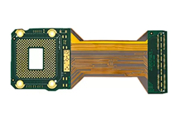
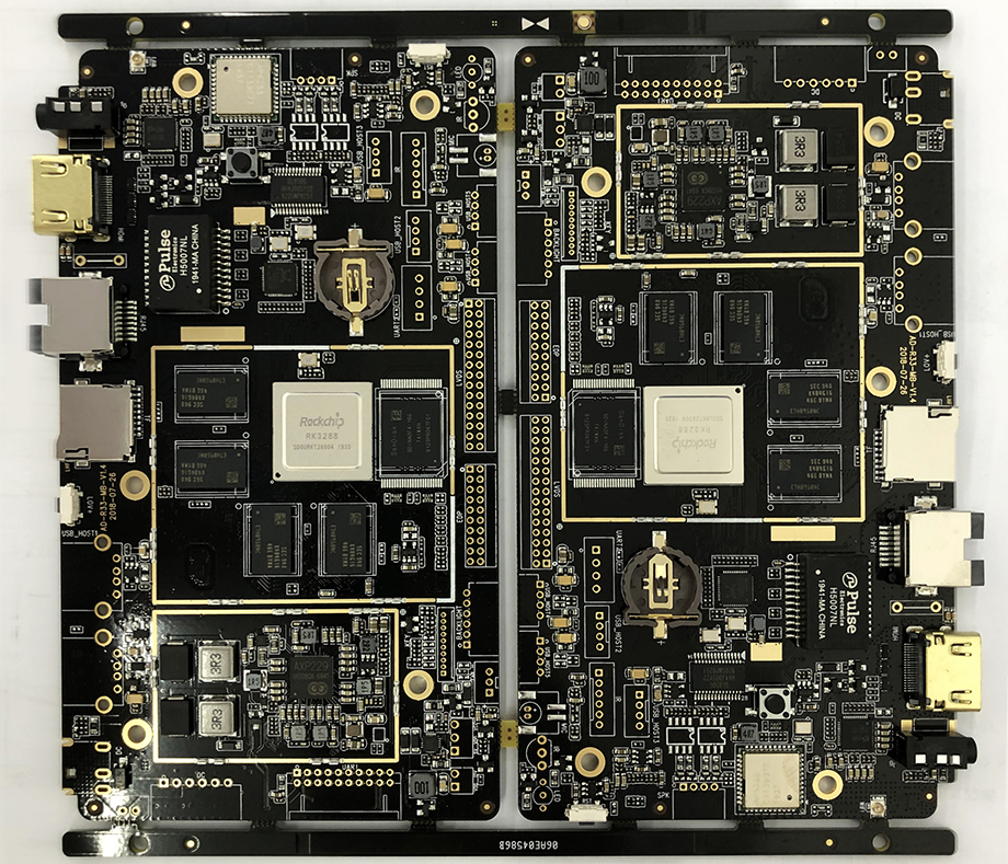
High-speed PCB design refers to the practice of designing high-speed signals on a printed circuit board (PCB). High-speed signals typically have rise and fall times of less than 1 nanosecond (ns). It encompasses knowledge in areas such as signal integrity, electromagnetic compatibility, impedance matching, layer stack-up design, and routing rules. The goal of high-speed PCB design is to ensure the quality and reliability of high-speed signals, avoiding issues like signal distortion, interference, and reflection.
Table of Contents
Factors to Consider in High-Speed PCB Design
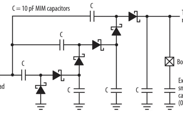
– Impedance Matching: High-speed signals generate electromagnetic fields during transmission. If the signal impedance does not match the transmission line impedance, signal reflection occurs, degrading signal integrity.
– Spacing: High-speed signals can be interfered with by other signals, power lines, and ground lines. Increasing the spacing between signals helps reduce interference.
– Length Matching: The two traces of a differential signal should have equal lengths. Length mismatch can cause signal skew, thereby reducing signal integrity.
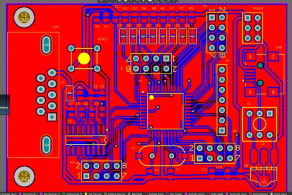
– Tools and Techniques: High-speed PCB design requires specialized tools and techniques to ensure signal integrity. These tools help designers analyze signal transmission paths and identify potential issues.
Applications of High-Speed PCB Across Various Fields
High-speed PCB technology is widely applied in various fields of electronics. Here are some specific examples:
– Digital Signal Processing (DSP): DSP refers to the technology of processing digital signals and is widely used in applications such as audio and video processing, image processing, and communication. High-speed PCB design is crucial in DSP applications, as DSP systems often require the transmission of high-speed signals. For instance, in audio and video processing systems, high-speed PCBs are used to transmit audio and video signals.
-Communication: Communication systems, such as Ethernet, fiber-optic communication, and wireless communication, often require the transmission of high-speed signals. High-speed PCB design plays a vital role in ensuring signal integrity and reliability in these systems.
– Storage: Storage systems, including solid-state drives (SSDs), memory, and flash storage, rely on high-speed PCB design to ensure fast and reliable data transmission. For example, in SSDs, high-speed PCBs are used to transmit data signals. Similarly, in memory and flash storage systems, high-speed PCBs facilitate data signal transmission.
– Image Processing: Image processing applications, such as digital cameras, scanners, and displays, depend on high-speed PCB design to transmit high-speed signals. For instance, in digital cameras, high-speed PCBs are used to transmit image signals. In scanners and displays, high-speed PCBs also play a critical role in image signal transmission.
Conclusion
High-speed PCB design is a complex task that requires extensive expertise. Through proper design and implementation, high-speed PCBs can effectively transmit signals and meet system requirements.