Table of Contents
Design points of golden fingers
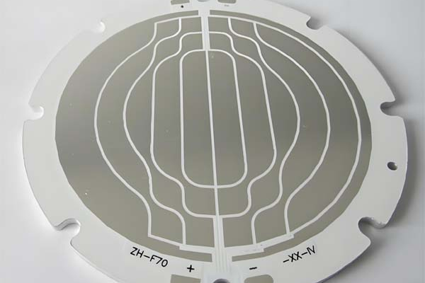
Gold Finger is a row of gold-plated conductive contacts designed on the edge of a printed circuit board (PCB), named after their surface being gold-plated and resembling fingers. It is the physical interface that enables electrical connection between PCB and other devices such as motherboard slots, expansion card interfaces, etc.So,how to make golden finger PCB?
1. Structural design of golden fingers
-Oblique (guide angle) design
The edge of the golden finger should be designed at 45 ° or other angles (such as 20 °, 30 °) to reduce friction damage when inserted into the slot. If not chamfered, the right angle is prone to scratching the slot, reducing reliability.
-Safe distance
The golden finger should maintain a safe distance of 0.6-1.5mm from the edge of the board to prevent damage to the coating during beveled edge treatment. The thickness range of the board is usually 1.2-2.4mm, and if it exceeds this range, it may not be possible to beveled it.

-Layout of long and short gold fingers
Main lead width of 40mil, secondary lead width of 20mil, connection points of 6mil, spacing of 8mil. When the leads enter the single board, they need to be connected diagonally or with rounded corners to avoid impedance jumps caused by right angles.
2. Electrical and solder mask design of Golden Finger
-Solder mask window
The golden finger area needs to be completely opened to avoid poor contact caused by solder mask ink residue. The window opening range should be 10mm larger than the edge of the board and kept at a distance from the surrounding copper skin to prevent copper exposure.

-Restrictions on surface copper plating
Copper plating is prohibited on the surface of the gold finger to avoid multiple identical network solder pads being connected as a whole, which may affect insertion and removal.
-Inner layer copper cutting treatment
The inner layer needs to be copper cut by at least 3mm to reduce the impedance difference between the gold finger and the impedance line, while enhancing ESD protection capability. Some designs (such as PCIe) require full copper cutting in the gold finger area.
3. Material and Coating Selection
-Electroplated hard gold
Thickness 3-50 μ m, containing nickel/cobalt alloy, high hardness (200+HV), strong wear resistance, suitable for high-frequency plugging scenarios (such as graphics cards, industrial equipment), but with high cost.
-Chemical immersion gold (ENIG)
thickness 1-3 μ m, smooth surface, low cost, suitable for low insertion and extraction frequency scenarios (such as consumer grade memory), but poor wear resistance.
The manufacturing process of golden fingers, how to make golden fingers?
1. Core process flow of Golden Finger
-Substrate treatment: Copper substrates are etched to form conductive contacts, followed by nickel plating as the bottom layer to improve adhesion and corrosion resistance.
-Gold plating process:
-Electroplating hard gold: By electrolytically depositing gold cobalt/gold nickel alloy, the thickness is controllable and suitable for local high wear resistance requirements.
-Chemical deposition of gold: forming a uniform gold layer through non current deposition, low cost, suitable for whole board processing.
-Diagonal cutting: precise guide angles are achieved using CNC milling machines or laser cutting, typically ranging from 20 ° to 45 °.

2. Special process requirements
-CAM compensation: The inner copper foil needs to be stacked according to the product type (80mil for ordinary products, 40mil for optoelectronic/memory products), with a lead width of 12mil and strict calibration of solder pad spacing.
-Anti oxidation treatment: Before gold plating, the copper surface needs to be thoroughly cleaned, and some processes introduce nitrogen gas protection to prevent oxidation.
Key considerations in the manufacturing process of golden fingers
1. Process control
-Consistency of plating thickness: When electroplating hard gold, it is necessary to ensure uniform thickness and avoid local thinning that may cause a decrease in wear resistance.
-Drilling accuracy: The aperture and depth should be consistent to avoid interference or damage to the PCB during insertion and removal.
2. Quality control
-Wear resistance test: High frequency insertion and extraction scenarios (such as PCIe) require ≥ 500 insertion and extraction tests to ensure that the coating does not peel off.
-DFM detection: Use tools such as Huaqiu DFM to detect design files in advance and avoid production risks. The cost of gold finger products is high, and it is necessary to strictly avoid rework of finished products.
3. Environment and operating standards
-Pollution prevention: It is forbidden to directly touch the golden fingers during operation to avoid surface contamination by oil or impurities.
-Storage and transportation: shockproof packaging is required to avoid damage to the coating caused by mechanical impact.
Comparison and Trends
-Alternative solution: Gold finger tin plating/silver has low cost but short lifespan; Emerging high-density connectors (such as LCP materials) are gradually being applied, but gold fingers still dominate the field of high reliability.
-Environmental trend: In the future, lead-free electroplating or renewable materials may be used to reduce environmental impact.
By optimizing design and process control, Goldfinger continues to play a critical role in high-frequency, high reliability electronic devices such as 5G and AI hardware.
The above is all about how to make golden finger PCB. If you have golden finger PCB requirements, you can contact us.