This blog mainly introduces what the golden finger is and its advantages.
Table of Contents
Definition:
Gold Finger is a row of gold-plated conductive contacts designed on the edge of a printed circuit board (PCB), named after their surface being gold-plated and resembling fingers. It is the physical interface that enables electrical connection between PCB and other devices such as motherboard slots, expansion card interfaces, etc.
Core role:
1. Electrical connection:
-As a channel for signal and power transmission, it connects the circuits on the PCB with external devices such as memory slots and graphics card slots.
-The gold plating layer provides low resistance and high conductivity, ensuring the stability of signal transmission.
2. Mechanical insertion and removal:
-Removable connection is achieved by inserting slots, supporting modular design (such as replacement of memory modules and graphics cards).
-The hardness and wear resistance of the golden fingers ensure the reliability of multiple insertions and removals.
3. High frequency signal support:
-The antioxidant properties and low skin effect of gold make it suitable for the transmission of high-frequency signals (such as PCIe 4.0, DDR5), reducing signal attenuation.
4. Environmental resistance:
-The gold layer is resistant to oxidation and corrosion, and can maintain long-term stability in harsh environments such as humidity and high temperatures.
What is a golden finger and what are its classifications
1. Classify by application scenario
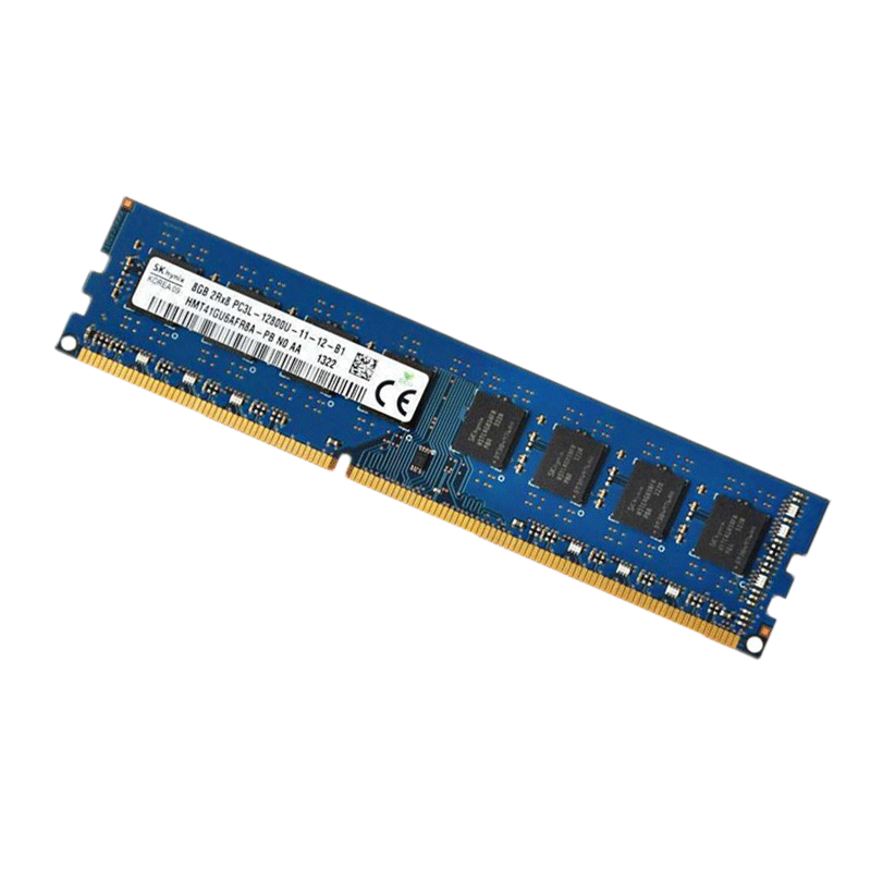
-Memory module gold finger:
-Like DDR4/DDR5 memory modules, with dense contacts and thin plating (chemical gold plating), they need to match the high-density design of motherboard slots.
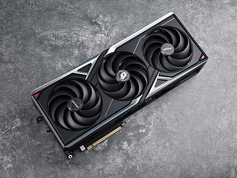
-Graphics card gold finger:
-Like PCIe interface, the contacts are wide and the coating is thick (electroplated with hard gold), supporting high-power transmission and high-speed signals (such as PCIe 5.0).
-Extended Card Gold Finger:
-Such as M.2 SSDs, network cards, sound cards, etc., usually adopt short and compact designs (such as the “golden finger” part of M.2).
-Industrial equipment golden finger:
-Used for industrial computers, communication equipment, etc., it requires stronger resistance to vibration and pollution.
2. Classified by structural design
-Through Hole:
-The golden finger is directly inserted into the slot and contacts through the spring plate inside the slot (such as a traditional PCI card).
-Surface Mount Technology (SMT):
-The golden finger is flush with the PCB surface and connected through precise alignment (such as high-speed backplane connectors).
3. Classified by plating process
-Electroplated Hard Gold:
-Coating thickness: 0.3-50 μ m (commonly 30 μ inches), containing nickel or cobalt alloy, high hardness (200+HV).
-Advantages: Strong wear resistance, suitable for high-frequency plugging and unplugging scenarios (such as graphics cards and industrial equipment).
-Disadvantages: High cost and complex process.
-Electroless Nickel Immersion Gold (ENIG):
-Coating thickness: 0.05-0.1 μ m, with nickel layer as the base and gold deposition on the surface.
-Advantages: Low cost, smooth surface, suitable for low-frequency, low insertion and extraction applications (such as some consumer grade memory).
-Disadvantages: Poor wear resistance, prone to poor contact due to insertion and removal wear.
4. Classify by functional signals
-Single function gold finger: only transmits a single signal (such as power or ground).
-Multi functional gold finger: integrates multiple signals (such as PCIe gold finger containing data, power, and clock signals).
The advantages of golden fingers
1. Excellent conductivity:
-The electrical resistivity of gold is extremely low (2.44 × 10 ⁻⁸Ω· m), reducing signal transmission loss and suitable for high-speed and high-frequency scenarios.
2. Super abrasion resistance:
-Hard gold coating (such as gold cobalt alloy) can withstand thousands of insertions and removals (such as PCIe specification requirement ≥ 500 times), with a long lifespan.
3. Anti oxidation and corrosion resistance:
-Gold hardly oxidizes at room temperature, avoiding poor contact of copper substrates caused by oxidation (compared to tin plating which is prone to oxidation).

4. Compatibility and Standardization:
-The size, spacing, and bevel angle of the golden fingers follow industry standards (such as PCI-SIG, JEDEC) to ensure interchangeability between devices.
5. High frequency signal integrity:
-The gold-plated surface is smooth, reducing signal reflection and impedance fluctuations, and supporting high-frequency transmission above 10 GHz (such as PCIe 6.0).
6. High mechanical strength:
-Nickel plated bottom layer enhances the mechanical strength of gold fingers, preventing deformation or fracture.
7. Environmental adaptability:
-It can maintain stable performance even in harsh environments such as high temperature, high humidity, and salt spray.
Application scenario examples
–Consumer electronics: memory modules, graphics cards M.2 SSD。
–Industrial field: PLC control modules, pluggable boards for communication base stations.
–Automotive electronics: Expansion interfaces for in car entertainment systems and ADAS modules.
Comparison with other connection methods
| characteristic | Goldfinger | Ordinary tin plated contacts | Spring needle connection |
| Conductivity | Excellent (gold-plated) | Generally (prone to oxidation) | Good (dependent on material) |
| wear resistance | Extremely strong (hard gold) | differ from | medium |
| High frequency performance | excellent | differ from | medium |
| cost | tall | low | medium |
| Plug and unplug lifespan | 500~1000 times | <100 times | 1000~5000 times |
Summarize
Gold fingers, with their gold plating layer’s conductivity, wear resistance, and oxidation resistance, have become the core solution in PCB connection technology, especially irreplaceable in high-frequency and high reliability scenarios. With the miniaturization and high frequency of electronic devices, the technology of gold fingers (such as thinner coatings and more precise beveled edge designs) will continue to be optimized to meet the needs of emerging fields such as 5G and AI computing. The above is all about what a golden finger is. If you want to learn more about PCB knowledge, you can contact us directly.