Table of Contents
Introduction: The Strategic Importance of PCB Layer Planning
In printed circuit board (PCB) design, determining the appropriate layer count represents one of the most critical decisions that impacts everything from signal integrity and thermal performance to manufacturing costs and production timelines. While increasing layer count can solve many design challenges, it also raises manufacturing expenses—sometimes significantly. This comprehensive guide explores the key factors that influence PCB layer count decisions, providing a structured framework to help engineers and designers strike the optimal balance between performance, reliability, and cost-effectiveness for their specific applications.
1.Understanding the Fundamental Trade-Offs
The Cost-Performance Dilemma
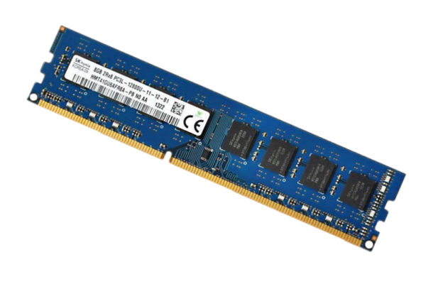
PCB layer count directly correlates with both manufacturing complexity and unit cost. As a general rule, each additional layer increases fabrication expenses due to additional materials, processing time, and yield considerations . While a 2-layer board represents the most economical option for simple circuits, modern electronic devices with complex components and stringent performance requirements often necessitate multilayer configurations .
The relationship between layer count and cost isn’t always linear. The price difference between 2-layer and 4-layer boards is typically more significant than between 6-layer and 8-layer configurations . Understanding these cost thresholds helps in making informed decisions during the early design phases.
Design Flexibility vs. Manufacturing Constraints
More layers provide greater routing flexibility and can simplify the layout process, potentially reducing design time for complex circuits . However, each additional layer introduces new manufacturing considerations, including layer-to-layer registration challenges and increased potential for defects . The most effective designs achieve their performance goals with the minimum number of layers that reliably meet all electrical and physical requirements.
2.Key Factors Influencing PCB Layer Count Decisions
1. Component Density and Escape Routing Requirements
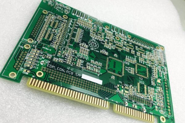
High-density components, particularly fine-pitch BGAs (Ball Grid Arrays), often dictate minimum layer count requirements based solely on escape routing patterns .
BGA pin pitch directly influences how many traces can be routed between adjacent vias:
•1.0mm BGA pitch: Typically allows two traces between vias, potentially requiring fewer layers for escape routing
•0.8mm BGA pitch: Generally permits only one trace between vias, typically necessitating additional layers for complete component fanout
•<0.5mm BGA pitch: Usually requires advanced techniques like blind and buried vias and additional dedicated signal layers
Before finalizing layer count, designers should perform a comprehensive BGA escape analysis to verify that all signals can be routed from dense components with the proposed layer stackup .
2. Signal Integrity Requirements
High-speed signals impose strict requirements on impedance control, crosstalk mitigation, and return path management—all of which influence layer count decisions .
Critical signal integrity considerations include:
•Impedance-controlled routing: Requires appropriate reference planes and dielectric spacing, typically needing dedicated signal layers adjacent to continuous reference planes
•High-speed signals: Best positioned between reference planes to contain electromagnetic fields and minimize radiation
•Signal layer-to-reference plane ratio: Maintaining a 1:1 ratio between signal layers and reference planes provides optimal signal quality but increases layer count
For designs with numerous high-speed buses or stringent EMC requirements, additional layers may be necessary to maintain proper signal integrity across all critical interfaces .
3. Power Delivery Network Complexity
The number of power domains and their current delivery requirements significantly impact power plane planning .
Power delivery considerations affecting layer count:
•Multiple voltage domains: Each primary power rail typically requires its own plane or dedicated copper area, potentially necessitating additional layers
•Current capacity: High-current paths may require thick copper weights or multiple parallel planes to avoid excessive voltage drop and heating
•Power integrity: Low-impedance power distribution often requires closely spaced power-ground plane pairs for effective decoupling
Mixed-signal designs with separate analog and digital power domains further increase power delivery complexity, often requiring additional layers to maintain proper isolation between domains .
4. Electromagnetic Compatibility (EMC) and Shielding
EMC performance is significantly influenced by layer stackup design, with proper planning often reducing the need for additional shielding components .
Effective EMC strategies affecting layer count:
•Shielded signal layers: Positioning critical signals between reference planes provides natural shielding
•Multiple ground planes: Using continuous ground planes on adjacent layers helps contain electromagnetic emissions
•Split-plane isolation: Sensitive circuits sometimes require isolated ground regions, potentially necessitating additional layers
Products targeting commercial markets with strict emissions standards often incorporate additional ground planes or shielded layer configurations to ensure compliance .
3.Practical Layer Count Determination Methodology
Step-by-Step Assessment Process
1.Component Analysis
–Identify all fine-pitch components (BGAs, connectors)
–Perform initial escape routing analysis for dense components
–Determine approximate signal layer requirements based on component fanout
2.Signal Inventory and Classification
–Count and categorize signals by type (high-speed, differential, sensitive analog)
–Identify signals requiring impedance control or special routing considerations
–Estimate signal layer needs based on routing density and signal types
3.Power Distribution Planning
–List all power rails and their current requirements
–Determine optimal power plane configuration
–Identify any power domains that can share layers
4.Board Size and Density Calculations
–Evaluate preliminary component placement and routing density
–Identify potential routing bottleneck areas
–Adjust layer count or board size to address congestion issues
5.Cost-Performance Optimization
–Evaluate layer count alternatives against budget constraints
–Consider design time savings from additional layers versus manufacturing cost increases
–Finalize layer count that meets all requirements with acceptable cost structure
Common Layer Count Configurations and Applications
Table: Typical PCB Layer Count Applications and Considerations
| Layer Count | Common Applications | Key Advantages | Design Considerations |
| 1-2 Layers | Simple circuits, consumer electronics, power supplies | Lowest cost, rapid fabrication | Limited routing space, challenging impedance control |
| 4 Layers | Most common count for complex designs, industrial controls, automotive systems | Good signal integrity capabilities, reasonable cost | Limited power planes, potential signal layer constraints |
| 6-8 Layers | Dense designs, multiple BGAs, advanced embedded systems | Excellent signal integrity, multiple power domains | Moderate cost increase, more complex fabrication |
| 10+ Layers | High-speed digital, complex communications, server motherboards | Optimal signal performance, comprehensive power delivery | Significant cost premium, extended lead times |
4.Advanced Considerations for Complex Designs
HDI Technologies and Their Impact
High Density Interconnect (HDI) technologies—including microvias, blind vias, and buried vias—can significantly reduce layer count requirements for designs with extremely dense components . While HDI processes increase fabrication cost per layer, they may enable a reduced overall layer count, potentially resulting in better overall performance in a thinner profile .
Material Selection and Performance
Dielectric materials influence signal propagation characteristics and layer stackup planning . High-speed designs often use specialized materials with controlled dielectric constants (Dk) and dissipation factors (Df), which may affect the achievable layer thicknesses and overall stackup configuration .

Thermal Management Considerations
Power dissipation requirements influence layer planning, particularly for designs with high-current components or stringent thermal requirements . Thermal vias, copper thickness, and plane layers all contribute to heat spreading—factors that may necessitate additional layers for adequate thermal management .
5.Cost Optimization Strategies
Right-Sizing Your Layer Count
The most cost-effective designs implement all required functionality with the minimum viable layer count . Strategies for optimizing layer count include:
•Careful floorplanning: Component placement that minimizes routing congestion
•Signal prioritization: Assigning critical signals to preferred layers while grouping less critical signals efficiently
•Power sharing: Implementing creative power distribution that minimizes dedicated power planes
•Utilizing both sides: Placing components on both top and bottom layers to reduce board area requirements
Prototyping and Iteration Approach
For uncertain or borderline designs, consider a phased approach :
1.Prototype with a conservative (higher) layer count to ensure functionality
2.Analyze the completed design for potential layer reduction opportunities
3.Optimize the production version with a refined layer count based on actual routing utilization
6.Future Trends and Evolving Considerations
Increasing Component Density
As component packages continue to shrink in size while increasing pin counts, layer count requirements for many applications are trending upward . Designs that previously worked well with 4 layers may now require 6 or more layers to accommodate modern component densities.
High-Speed Signaling Advances
Emerging interface standards with higher data rates and stricter signal integrity requirements are driving more sophisticated layer stackups with carefully controlled impedance characteristics . This often translates to additional reference planes and dedicated signal layers for critical interfaces.
Conclusion: A Methodical Approach to Layer Count Decisions
Determining the optimal PCB layer count requires careful consideration of multiple technical and economic factors. By systematically evaluating component requirements, signal integrity needs, power distribution complexity, and cost constraints, designers can arrive at a layer count that delivers the required performance without unnecessary expense.
The most successful designs emerge from an iterative process that balances competing priorities while maintaining focus on the product’s core requirements. With the structured approach outlined in this guide, engineering teams can make informed PCB layer count decisions that result in reliable, manufacturable, and cost-effective products.
Remember that while increasing layer count solves many design challenges, the most elegant solution often achieves the desired performance with the simplest possible implementation.