Against the backdrop of the popularization of 5G communication, AI computing, and high-speed interfaces such as PCIe 4.0 and USB 3.2, four layer PCBs have become the mainstream choice for mid to high end electronic products due to their high cost-effectiveness and balanced electromagnetic compatibility (EMC). However, the wiring of high-speed signals (>5GHz) needs to balance impedance control, crosstalk suppression, and timing synchronization. This article combines industry practice and simulation data to systematically explain the core strategies for optimizing high-speed signals on four layer boards.
Table of Contents
1、 Stacked structure and material selection: laying the foundation for performance
1. Golden layered architecture
It is recommended to adopt the signal ground power signal (Top GND PWR Bottom) stacking scheme, which has the advantages of:
-The signal layer is adjacent to the reference plane (GND/PWR), shortening the return path and reducing radiation (measured EMI reduced by 40%);
-The power layer and geological layer form a planar capacitor (typical value 10-20pF) to suppress power noise.

Example: In a certain DDR4 design, high-speed data lines are arranged in the top layer, and the GND layer is shrunk by 20mil to form an isolation band, resulting in a 35% improvement in signal integrity.
2. Material parameter matching
-Dielectric constant (Dk): Rogers 4350B (Dk) is selected for high-frequency signals (>10Gbps)= 3.66@10GHz )For regular signals (<5Gbps), FR-4 (Dk=4.5) is used;
-Loss factor (Df): In high-speed scenarios, Df<0.005 is required to avoid signal attenuation (such as the insertion loss of PCIe 4.0, which needs to be<0.3dB/inch).
2、 Impedance control and differential pair design: ensuring signal purity
1. Impedance continuity management
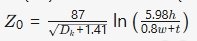
-Transmission line type: Microstrip is used for surface wiring, and Stripe is used for inner wiring. Impedance is calculated using SI9000 ,formula:
-Compensation measures: Add a back drill at the through-hole to eliminate residual piles and compensate for a length error of ± 5ml.
2. Differential pair wiring golden rule
-Equal length and equal distance: USB 3.0 differential pair with a line width of 10 mil and a line spacing of 6 mil, with a length error of less than 5 mil, to avoid common mode noise;
-Shielding strategy: Arrange ground hole arrays on both sides of the differential pair (spacing ≤ 100mil), and adopt a grounded design (GND protection line spacing 3W).
3、 Equal length routing and timing optimization: eliminating timing deviation
1. Serpentine routing and topological structure
-Compensation geometry: Single winding spacing ≥ 3 times the line width to avoid impedance mutations; DDR5 address lines adopt Fly by topology, with branch length differences<10%;
-Length matching tool: Use Cadence Sigrity for Delta-L analysis and dynamically adjust the routing bend position.

2. Cross layer transition optimization
-Via layout: When changing layers for high-speed signals, add ground holes (spacing ≤ 200mil) to adjacent layers to reduce impedance jumps;
-Reference plane continuity: To avoid wiring in the dividing plane, different power domains need to be connected through splicing capacitors (10-100nF).
4、 Power Integrity (PI) and EMC Collaborative Design
1. Decoupling capacitor network
-Multi level filtering: Place a 0.1 μ F (high frequency)+10 μ F (low frequency) capacitor combination on the power pin of the DDR chip to form a 20MHz-1GHz broadband filter;
-Current path optimization: The power plane segmentation should follow the principle of “minimum return path”, with adjacent segmentation spacing ≥ 0.5mm.
2. EMI suppression measures
-Edge protection: A protective ring is formed by extending 20mil beyond the ground plane, and grounding vias are arranged every 1/20 wavelength;
-Shielding layer design: Four layers of shielding (Top GND Signal Bottom) are used for RF signal lines, increasing insertion loss by 20dB.
5、 Verification and Mass Production Assurance
1. Multi dimensional simulation verification
-SIwave simulation: Analyze impedance fluctuations of non ideal structures such as vias and connectors (target deviation<± 7%);
-Eye diagram test: Verify USB 3.0 signal eye height (≥ 80% VDD) and jitter (<50ps RMS) through Keysight oscilloscope.

2. Design for Manufacturability (DFM)
-Line width/line spacing: Recommended for mass production is 6mil line width+8mil line spacing, and tear drop pads are used in the BGA area;
-Splicing strategy: V-cut avoids high-speed signal areas to prevent mechanical stress from causing microcracks.
Conclusion
The high-speed signal design of a four layer PCB is a system engineering that requires collaboration throughout the entire process, from stack planning, impedance control to verification testing. Through precise simulation driving and process optimization, signal integrity, power integrity, and EMC balance can be achieved under controllable costs. In the future, with the surge in bandwidth demand for AI chips, the design of four layer boards will rely more on 3D electromagnetic field simulation and AI assisted wiring tools, driving PCB design into a new stage of “intelligent optimization”.