>The global AC-DC power chip market is expected to expand at a compound annual growth rate of 8.22%, surpassing RMB 176.2 billion by 2030- and high reliability PCB design is becoming a key winner in improving power efficiency.
In the wave of miniaturization and efficiency of electronic devices, AC-DC power supply serves as the core hub for energy conversion, and its performance directly affects the reliability from mobile phone chargers to data center servers. As the physical foundation for carrying power chips, power devices, and circuit connections, the design quality of PCB determines the conversion efficiency, heat dissipation capacity, and electromagnetic compatibility of power modules.
This article will deeply analyze the technical value of PCB in AC-DC power supply, from basic principles to cutting-edge trends, providing engineers with practical design guidelines.
Table of Contents
1、 AC-DC power supply: the energy conversion core of modern electronic devices
Basic working principle
The core task of AC-DC power supply is to convert alternating current (AC) into direct current (DC). This process typically involves four key stages:
1. Transformer voltage reduction: Reduce high-voltage alternating current (such as 220V AC) to the applicable voltage through the iron core and winding.
2. Rectification conversion: AC power is converted into pulsed DC power by diodes or rectifier bridges. Common topologies include flyback, half bridge, and active clamp architectures.
3. Filtering and smoothing: Using capacitors and inductors to construct a low-pass filter, eliminating voltage ripple and ensuring smooth current output.
4. Voltage stabilization control: Real time voltage regulation is achieved through feedback loops (such as optocoupler isolation) to keep the output stable in load fluctuations, with an accuracy of ± 1%.
Market Application and Growth
The global market size of AC-DC power chips has reached 109.7 billion yuan in 2024, and is expected to exceed 176.2 billion yuan by 2030, with a compound annual growth rate of 8.22%. Consumer electronics (chargers/home appliances) account for over 60%, with significant growth in industrial and automotive electronics.
2、 Three key roles of PCB in AC-DC power supply
1. Accurate implementation of electrical connections
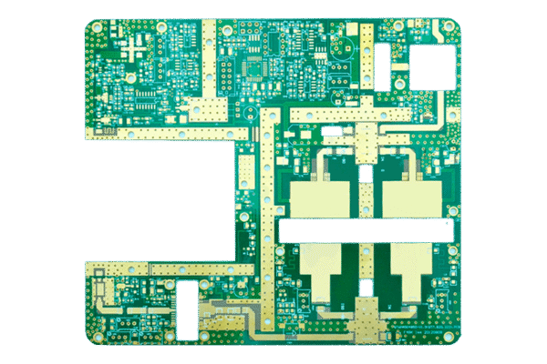
PCB carries high-density circuits through multi-layer copper foil wiring (2-16 layers):

-High voltage and low voltage isolation: The input stage (85-265V AC) and output stage (5-48V DC) adopt a partitioned layout to avoid breakdown caused by insufficient creepage distance.
-Optimization of high current path: The line width from the rectifier bridge to the primary line of the transformer should be ≥ 2mm, increasing the current carrying capacity by 30% and reducing conduction losses.
Case: Dongke Semiconductor DK3718AD encapsulated gallium nitride chip achieves 98% ZVS (zero voltage switching) efficiency through PCB embedded heat dissipation holes.
2. The core carrier of heat dissipation management
-Integrated heat sink design: MOSFET and rectifier tube are soldered to PCB, and heat is conducted to the metal substrate (such as aluminum PCB) through 2oz thick copper foil and heat dissipation via holes, resulting in a temperature drop of up to 10 ℃.
-Partition heat dissipation strategy: Copper surface heat sinks (Thermal Pad) are laid in the switch tube area, while ordinary FR-4 is used in the control chip area, balancing cost and performance.
3. The decisive link in electromagnetic compatibility (EMC)
-Noise suppression structure: The combination of common mode inductor and X/Y capacitor at the input can attenuate common mode noise by more than 30dB.
-Ground wire segmentation technology: As shown in patent CN202565176U, the power ground (GND1), detection ground (GND2), and control ground (GND5) are connected at a single point at the input capacitor, reducing conducted radiation noise by 50%.
3、 Key points of PCB design: balancing performance and reliability
The AC-DC power PCB needs to meet safety regulations, thermal management, and signal integrity requirements simultaneously. The following are the key design specifications:
1. Safety distance design
| Voltage level | Creepage distance | Electrical clearance |
| ≤300V | ≥2.5mm | ≥1.5mm |
| 300-600V | ≥3.2mm | ≥2.0mm |
Complies with IEC62368 standard to avoid high voltage discharge risks
2. Ground wire segmentation and single point connection
-Partition plane: The power ground and signal ground are separated by slotting, and only connected at a single point on the negative pole of the input capacitor to avoid coupling switch noise to the control circuit.
-Zero impedance path: The high current return path prohibits right angle wiring and uses an arc or 45 ° angle to reduce skin effect losses.
3. Thermal management design
-Power device layout: The switch tube and rectifier tube should be kept away from the electrolytic capacitor (the lifespan is halved for every 10 ℃ temperature rise), and the recommended distance should be ≥ 5mm.
-Thermal conduction channel: Arrange heat dissipation vias (aperture ≥ 0.3mm, spacing 1mm) in an array at the bottom of the MOSFET, and fill them with thermal conductive paste to connect to the bottom copper surface.
4. Loop control and EMI suppression
-Minimize the three key loops:
① Input circuit (rectifier bridge input capacitor)
② Switching circuit (transformer switch tube)
③ Output circuit (rectifier tube output capacitor)
A loop area of<1cm ² can reduce radiated noise by 15dB.
-Shielding technology: Install Guard Ring (grounding copper ring) around the transformer to absorb leakage magnetic flux.
4、 Future trend: PCB innovation towards high power and high frequency
1. High power density design
-Application of Gallium Nitride Encapsulation Chip: For example, Dongke DK065G encapsulates GaN devices with control ICs, increasing the switching frequency to 1MHz and reducing the PCB area by 40%.
-Stacked PCB: The main power layer and control layer are vertically interconnected, achieving a power density of 10W/cm ³ like TDK Lambda ZWS150B (38% higher than traditional solutions).
2. Popularization of high-frequency materials
-PTFE substrate (dielectric constant 2.2): used for LLC resonant circuits above 100W, with signal loss 60% lower than FR-4.
-Ceramic filling material: with a thermal conductivity of 4W/(m · K), it is suitable for the high temperature resistance requirements of on-board OBC modules.
3. Digital control integration
-Intelligent power chip: such as MPS HR1211 digital controller, dynamically configuring PFC parameters through UART interface embedded in PCB, increasing efficiency to 96%.
-The demand for AI server PCBs has exploded: the market size is expected to reach 7.9 billion yuan by 2025, requiring PCBs to support 40Gbps high-speed differential signals (loss ≤ 0.5dB/inch).
Conclusion: PCB – the invisible engine of AC-DC power evolution
With the acceleration of global electrification, AC-DC power supplies are evolving towards high-frequency, digital, and green directions. As the cornerstone supporting this transformation, PCB design needs to simultaneously break through three major capabilities:
-High reliability: meets the 0DPPM defect standard of IATF 16949 automotive grade certification;
-High integration: achieve blind buried hole stacking of more than 20 layers through HDI technology;
-Thermal electric collaborative design: using simulation tools to optimize thermal distribution and impedance matching.
>SysPCB has been deeply involved in PCB manufacturing for 18 years, providing:
>AC-DC specialized sheet solution: one-stop supply of high Tg FR-4, aluminum substrate, and high-frequency PTFE substrate
>- Free DFM analysis: Submit Gerber files and receive safety/cooling/EMC optimization suggestions within 48 hours
>Quick sampling service: 24-hour delivery of 6-20 layer boards, supporting 1000V high voltage testing
Get exclusive PCB quotation: fill out the form or send an email directly, and we will provide you with a quote service within 24 hours. Enjoy free DFM optimization and a 10% discount on SMT patches for your first order!