Table of Contents
Executive Summary
Signal Integrity (SI) represents one of the most critical considerations in modern high-speed printed circuit board (PCB) design and manufacturing. As digital signal speeds continue to accelerate—with contemporary systems now operating well beyond 50MHz where SI issues become significant—maintaining clean, accurate signals throughout transmission paths has become increasingly challenging . Signal integrity encompasses a series of quality metrics that ensure electronic signals propagate from transmitters to receivers without excessive distortion, timing errors, or quality degradation . This comprehensive guide explores the fundamental concepts, primary challenges, analytical methodologies, and practical mitigation strategies that PCB designers and engineers must master to develop reliable high-speed electronic systems capable of meeting the demands of today’s increasingly fast digital interfaces.
1.Understanding Signal Integrity: Fundamental Concepts
1.1 What is Signal Integrity?
Signal Integrity (SI) fundamentally refers to the quality and fidelity of an electrical signal as it travels from a transmitter to a receiver along any transmission path, which may include conventional metal traces, optical devices, or other media . In ideal digital systems, signals would maintain perfect rectangular waveforms with clean, sharp transitions between logical states. However, in physical implementations, all real-world signals—though representing digital values—are inherently analog in nature and consequently susceptible to various forms of degradation, including noise, distortion, and loss .

A signal is considered to have good integrity when it reaches the receiving component with the necessary voltage level at the required time while maintaining sufficient stability to be correctly interpreted . When signals fail to meet these criteria, systems may experience intermittent failures, timing violations, or complete functional breakdowns. Signal integrity engineering has thus emerged as a specialized discipline focused on analyzing, predicting, and mitigating the various factors that compromise signal quality across all levels of electronic packaging and assembly, from integrated circuit interconnections to PCB layouts .
1.2 The Growing Importance of SI in Modern Electronics
Several converging technological trends have elevated signal integrity from a niche concern to a fundamental design consideration:
•Increasing Signal Speeds: As semiconductor technology advances, signal switching frequencies continue to rise, with corresponding decreases in rise and fall times that exacerbate transmission line effects . Contemporary interfaces now commonly operate at gigabit-per-second data rates, where even nanosecond-scale distortions can cause significant bit errors .
•Board Miniaturization: The ongoing trend toward smaller form factors and higher component densities results in more compact layouts that can increase electromagnetic coupling between adjacent signals . This heightened proximity raises susceptibility to crosstalk and other interference-related issues.
•System Complexity: Modern electronic systems incorporate multiple high-speed interfaces operating simultaneously within constrained environments, creating complex interactions between signals, power delivery networks, and electromagnetic fields that must be carefully managed .
These factors collectively explain why signal integrity considerations have become indispensable in contemporary PCB design, particularly for applications such as 10 Gigabit Ethernet , high-speed memory interfaces , and other data-intensive systems where timing margins are increasingly constrained.
2.Primary Signal Integrity Challenges
2.1 Reflection and Impedance Mismatch
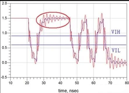
Signal reflections occur when impedance discontinuities along a transmission path cause portions of a signal to bounce back toward its source. These reflections interfere with the original signal, creating ringing (oscillations at signal transitions) and potentially causing false triggering of digital circuits . Key sources of impedance discontinuities include:
•Improperly Terminated Transmission Lines: When transmission lines lack matched termination at both source and load ends, energy reflects at the impedance boundaries .
•Via Transitions: The inherent stub effects and characteristic impedance changes at vias create discontinuities, particularly in high-density interconnects .
•Connector Interfaces: Variations in geometry and materials at connector junctions often introduce impedance mismatches .
•Changes in Trace Geometry: Sudden alterations in trace width or layer transitions modify characteristic impedance .
The impact of reflections becomes increasingly severe at higher frequencies, where the physical dimensions of discontinuities approach significant fractions of signal wavelengths, making proper impedance control throughout the signal path essential for maintaining signal integrity .
2.2 Crosstalk and Electromagnetic Coupling
Crosstalk represents one of the most pervasive signal integrity challenges in high-density PCB layouts, referring to the unwanted transfer of energy between adjacent transmission lines through electromagnetic coupling . This phenomenon manifests in two primary mechanisms:
•Capacitive Coupling: Resulting from electric fields between adjacent conductors, capacitive coupling induces voltage spikes on victim lines when aggressor signals transition .
•Inductive Coupling: Arising from magnetic fields generated by changing currents, inductive coupling introduces current fluctuations in nearby circuits .
Several key factors influence crosstalk magnitude, including:
•Signal Edge Rates: Faster transition times (shorter rise/fall times) significantly increase crosstalk, often making modern devices with rapid switching more problematic than older, slower technologies even at similar clock frequencies .
•Parallel Run Length: Longer adjacent trace segments allow more energy transfer, approximately proportional to coupling length .
•Inter-Trace Spacing: Crosstalk decreases non-linearly with increasing separation, with the most dramatic improvements occurring with initial spacing increments .
•Reference Plane Proximity: The dielectric thickness between signal layers and adjacent reference planes affects coupling, with thinner dielectrics typically reducing crosstalk .
Table: Comparative Crosstalk Characteristics for Different Transmission Line Configurations
| Transmission Line Type | Typical Crosstalk Performance | Key Controlling Factors |
| Microstrip | Moderate | Dielectric thickness, trace separation |
| Stripline | Superior | Dielectric thickness above and below, trace separation |
| Asymmetric Stripline | Good | Proximity to nearer plane dominates |
| Edge-Coupled Differential Pair | Controlled | Consistent spacing, differential impedance |
2.3 Power Integrity and Simultaneous Switching Noise
Power distribution network (PDN) performance has emerged as a critical aspect of overall system signal integrity. When multiple output buffers switch simultaneously, they draw large, rapid current surges from the power delivery system, potentially causing momentary voltage droops known as simultaneous switching noise or ground bounce . These power supply fluctuations can corrupt signals, reduce noise margins, and cause false switching. Key aspects include:
•PDN Impedance: The power delivery system must present low impedance across a broad frequency range to supply charge quickly during switching events .
•Decoupling Strategy: Proper selection and placement of decoupling capacitors helps maintain stable power delivery by providing localized charge reservoirs .
•Return Path Design: Continuous, low-impedance return paths for high-frequency signals are essential, as return current tends to flow primarily directly beneath signal traces in adjacent reference planes .
2.4 Loss Mechanisms and Dispersion
As signal speeds increase into the multi-gigabit range, frequency-dependent losses become increasingly significant:
•Dielectric Loss: Resulting from the PCB substrate material’s inherent dissipation factor, dielectric loss increases proportionally with frequency and can dominate total losses at higher speeds .
•Conductor Loss: Caused by trace resistance and the skin effect—where high-frequency currents concentrate near conductor surfaces, effectively reducing cross-sectional area and increasing resistance .
•Surface Roughness: Increased electron scattering on roughened copper surfaces further exacerbates conductor losses at high frequencies .
These loss mechanisms not only reduce signal amplitude but also cause dispersion, where different frequency components of a signal propagate at different velocities, resulting in waveform distortion that is particularly problematic for broadband digital signals .
2.5 Timing-Related Issues
Signal timing represents another critical dimension of signal integrity, with several potential failure mechanisms:
•Propagation Delay: The finite time required for signals to travel from transmitters to receivers .
•Skew: Differential timing between related signals, such as clock-data pairs or multiple bits within a parallel bus, which can cause sampling errors .
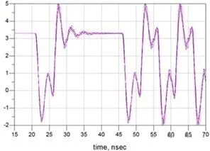
•Jitter: Timing variations in signal transitions, categorized as random or deterministic, that reduce timing margins and increase bit error rates .
These timing uncertainties become increasingly problematic as data rates increase and unit intervals decrease, making careful timing analysis an essential component of comprehensive signal integrity validation .
3.Signal Integrity Analysis Methodologies
3.1 Simulation Approaches
Modern signal integrity analysis relies heavily on predictive simulation throughout the design process:
•Pre-Layout Simulation: Conducted before detailed PCB layout to establish design rules, stackup configurations, and termination strategies . This includes interconnect planning and “what-if” analyses to determine optimal implementation approaches.
•Post-Layout Simulation: Performed after physical layout completion to verify that implementation adheres to signal integrity requirements . This stage incorporates precise trace geometries, via models, and actual component placements to identify potential issues requiring layout revisions.
•Topology Analysis: Evaluation of different networking approaches (point-to-point, multi-drop, T-tree, etc.) to determine optimal signal distribution architectures for specific applications .
These simulation methodologies employ sophisticated electromagnetic solvers that extract parasitic parameters and model transmission line effects, with accuracy dependent on the quality of component models such as IBIS (I/O Buffer Information Specification) for digital interfaces .
3.2 Modeling and Measurement Techniques
Accurate signal integrity analysis requires high-fidelity models of all system components:
•Transmission Line Modeling: Using tools like TDR (Time Domain Reflectometry) to characterize impedance profiles and identify discontinuities .
•Component Behavioral Modeling: IBIS models provide detailed I/V and V/T data without revealing proprietary semiconductor process information, enabling accurate simulation of device behavior under various loading conditions .
•S-Parameter Characterization: Frequency-domain models that comprehensively describe multi-port network behavior, particularly valuable for modeling connectors, cables, and PCB channels at high frequencies .
Validation through physical measurement remains essential, with advanced oscilloscopes and signal integrity analysis software enabling detailed characterization of eye patterns, jitter, and other quality metrics . The correlation between simulation predictions and actual measurements provides confidence in design processes and helps refine models for future projects .
4.Practical Mitigation Strategies
4.1 Impedance Control Techniques
Maintaining consistent characteristic impedance throughout the signal path is fundamental to minimizing reflections:
•Proper Termination Strategies: Selecting appropriate termination schemes (series, parallel, Thevenin, or AC) matched to the specific application and topology .
•Stackup Design: Careful planning of layer arrangements and dielectric thicknesses to achieve target impedance values while considering manufacturability and cost .
•Via Optimization: Minimizing via stub effects through back-drilling or using blind/ buried vias, with careful attention to antipad dimensions and return path continuity .
•Transition Management: Smoothing impedance changes at connectors, package boundaries, and layer transitions through compensatory geometries .
4.2 Crosstalk Reduction Methods
Effective crosstalk mitigation employs multiple complementary approaches:
•Strategic Spacing: Maintaining sufficient clearance between adjacent traces, with at least 3 times the dielectric height between critical signals for significant crosstalk reduction .
•Guard Traces: Placing grounded traces between aggressor and victim signals to provide additional isolation, though effectiveness varies with frequency and implementation .
•Differential Signaling: Using balanced differential pairs for critical signals, providing inherent common-mode noise rejection and reduced electromagnetic emissions .
•Orthogonal Routing: Arranging adjacent signal layers with perpendicular routing directions to minimize overlap and coupling between layers .
•Shielding: Implementing ground planes between signal layers to contain electromagnetic fields, with stripline configurations typically offering superior performance to microstrip .
4.3 Loss Management Approaches
Addressing signal attenuation requires multiple strategies tailored to specific loss mechanisms:
•Material Selection: Choosing low-loss dielectric materials (with lower dissipation factors) for critical high-speed signals, particularly in multi-gigabit systems .
•Equalization Techniques: Implementing pre-emphasis (transmit-side equalization) or equalization (receive-side compensation) to counteract frequency-dependent losses .
•Trace Geometry Optimization: Using appropriately wide traces to minimize DC resistance while considering the impact on routing density .
4.4 Power Integrity Enhancement
Robust power delivery system design is integral to overall signal integrity:
•Comprehensive Decoupling: Implementing a mix of bulk, ceramic, and sometimes specialty capacitors distributed throughout the PCB to maintain low PDN impedance across frequency .
•Planar Capacitance: Utilizing the inherent capacitance between closely spaced power and ground planes for high-frequency decoupling .
•Minimizing Loop Inductance: Designing power delivery paths with minimal inductance through short, wide interconnections and multiple vias .
5.Advanced Signal Integrity Considerations
5.1 Emerging Challenges in High-Speed Design
As data rates continue to escalate toward 224 Gbps and beyond, new signal integrity challenges emerge:
•Dielectric Material Limitations: Traditional FR-4 materials become increasingly lossy at higher frequencies, driving adoption of specialized laminates with superior high-frequency characteristics .
•Connector and Cable Effects: Interconnect systems between PCBs and subsystems introduce additional discontinuities and losses that must be carefully characterized and managed .
•System-Level Interactions: Complex interactions between signal integrity, power integrity, and electromagnetic compatibility require holistic analysis approaches .
5.2 Design for Manufacturing (DFM) Considerations
Successful high-volume production requires balancing performance objectives with manufacturability:
•Tolerance Analysis: Accounting for manufacturing variations in dielectric thickness, copper width, and material properties during simulation .
•Testability Implementation: Incorporating appropriate test points and access features to facilitate validation and troubleshooting without compromising signal integrity .
•Design Margin Allocation: Providing sufficient performance headroom to accommodate normal process variations while maintaining system functionality .
6.Conclusion
Signal integrity has evolved from a specialized concern to a fundamental discipline within high-speed PCB design, encompassing a comprehensive set of analysis techniques, mitigation strategies, and verification methodologies. As digital systems continue to push speed and density boundaries, the importance of robust signal integrity practice only increases.
Successful implementation requires a systematic approach addressing the entire signal path—from transmitter to receiver—with careful consideration of reflections, crosstalk, losses, and power delivery. By employing appropriate simulation tools throughout the design process, adhering to established layout practices, and validating performance through measurement, designers can develop complex systems that reliably meet their performance targets.
The future of signal integrity will undoubtedly present new challenges as data rates continue their upward trajectory, but the fundamental principles of proper termination, controlled impedance, electromagnetic containment, and comprehensive analysis will remain relevant regardless of specific technologies or applications.
Partner with Us for Your High-Speed PCB Design Requirements
Our expertise in signal integrity analysis and advanced PCB manufacturing ensures that your high-speed designs achieve optimal performance and reliability. With specialized capabilities in impedance control, EMI mitigation, and thermal management, we deliver PCB solutions that meet the stringent demands of modern digital systems.
Contact us today to discuss how we can support your next-generation projects with cutting-edge PCB technology tailored for your specific application requirements.