In high-speed digital circuit design, signal integrity (SI) is the core goal of ensuring that signals maintain waveform stability and timing accuracy during transmission. With the increase of chip operating frequency and PCB wiring density, problems such as signal reflection, crosstalk, and timing misalignment are becoming increasingly prominent. The following systematically elaborates on the key measures to ensure signal integrity from three dimensions: design strategy, technical means, and verification methods.
Table of Contents
1、 Basic design strategy: global planning from schematic to layout
1. Impedance control and transmission line design
The root cause of signal integrity issues lies in the mismatch of transmission line impedance. Impedance control during design should be achieved through the following methods:
-Material selection: Low dielectric constant (Dk) and high stability materials (such as Rogers 4350B) are used to reduce signal attenuation.

-Optimization of routing parameters: According to the formula
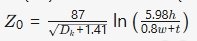
(where H is the dielectric thickness, W is the line width, and T is the copper thickness), accurately calculate the line width and spacing to ensure single ended impedance matching of 50 Ω or differential impedance matching of 100 Ω.
-Terminal matching: Add a series resistor (such as 29.9 Ω) or a parallel capacitor (such as 10pF) at the receiving end to suppress reflection; Differential signals can be obtained using a Thevenin terminal (69.8 Ω parallel 12pF).
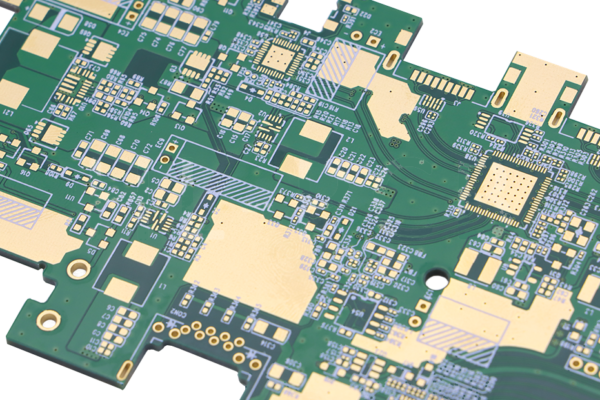
2. Stacked structure and power integrity

-Power/ground plane layout: Adopting a 4-layer or 6-layer board structure, the power layer is adjacent to the ground layer to shorten the return path. For example, sandwiching the high-speed signal layer between two ground planes can reduce radiation and crosstalk.
-Decoupling capacitor configuration: Place a combination of 0.1 μ F and 10 μ F capacitors near the chip power pin to form a low-frequency to high-frequency filtering network, suppressing ground bounce.
2、 Key technical means: wiring and electromagnetic compatibility optimization
1. Wiring rules and crosstalk suppression
-3W principle: The distance between adjacent signal lines should be ≥ 3 times the line width to reduce capacitive coupling. For high-speed buses such as DDR4, data lines and address lines need to be routed orthogonally to avoid parallel coupling.
-Avoid right angle wiring: Change the 90 ° corner to a 45 ° oblique or curved transition to reduce impedance transients. Tests have shown that right angle wiring can increase insertion loss by 0.5dB.
-Ground handling: Ground wires are laid on both sides of sensitive signals (such as HDMI TMDS) and connected to the planar layer through vias to isolate interference sources.
2. Timing management and signal synchronization
-Equal length cabling: Serpentine routing is used for bus systems (such as PCIe) to ensure that the length difference of each signal path is controlled within ± 5ml, avoiding timing misalignment. For example, the GT bank of Xilinx FPGA requires an equal length tolerance of ≤ 3mil.
–Pre emphasis and equalization: Enhance high-frequency components at the transmitting end (pre emphasis), and use continuous time linear equalization (CTLE) at the receiving end to compensate for transmission line losses.

3、 Validation and Iteration: Simulation Driven Design Closed Loop
1. Multi dimensional simulation analysis

-SIwave/ADS simulation: Establish a 3D electromagnetic model to analyze the impedance characteristics of non ideal structures such as vias and connectors. For example, the parasitic inductance of via holes can reach 1nH, and the impact needs to be reduced by back drilling or adding ground holes.
-Eye diagram test: Quantify signal quality through eye height and eye width, with target values meeting JEDEC standards (such as LPDDR5 requiring eye height ≥ 80% VDD).
2. Actual testing and DFT design
-T-probe testing: Set test points at the edge of the PCB, use a vector network analyzer (VNA) to measure S parameters, and verify transmission line losses and crosstalk.
-Boundary Scan (JTAG): Embedded with testability circuitry, real-time monitoring of signal waveforms, and rapid localization of faulty nodes.
4、 Typical case: High speed DDR5 memory wiring practice
In the design of a server motherboard, the DDR5 data rate reaches 6400MT/s, facing the following challenges:
1. Impedance fluctuation: Using SI9000 to calculate differential impedance, adjust the linewidth from 8mil to 7mil, reduce the dielectric thickness from 32mil to 24mil, and ultimately reduce the impedance deviation from ± 10% to ± 5%.
2. Crosstalk control: Insert a shielded ground wire between the DDR5 address line and clock line to reduce crosstalk noise from -35dB to -50dB.
3. Time series convergence: Using HyperLynx time series analysis tool, optimize the matching of trace length, and increase the establishment/holding time margin from 120ps to 250ps.
Conclusion
Signal integrity design is a system engineering that needs to be integrated throughout the entire process of schematic, layout, simulation, and testing. By combining impedance control, crosstalk suppression, timing optimization, and simulation verification, PCB reliability can be significantly improved. In the future, with the popularization of AI chips and optical communication technology, signal integrity design will rely more on multi physics simulation and intelligent optimization algorithms, promoting PCB design into the era of “zero defects”.