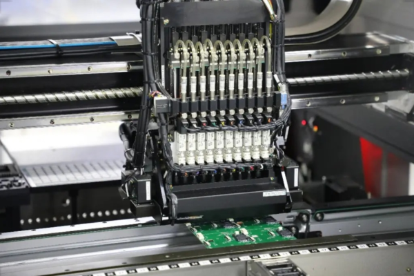
In the era of the Internet of Things, PCB antenna, as the “invisible wings” of electronic devices, are driving a wave of innovation in intelligent hardware through miniaturized design. This antenna structure, which is directly etched onto printed circuit boards, has become a standard component for consumer electronics products such as Bluetooth earphones and smartwatches due to its low cost and high integration.
Table of Contents
1、 Electromagnetic Art in the Microscopic World
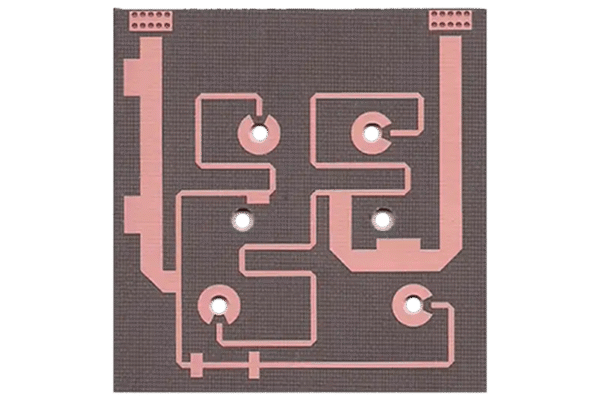
The core of PCB antenna is to convert electromagnetic wave energy into circuit signals. Unlike traditional external antennas with three-dimensional structures, planar inverted F antennas (PIFA) and meander lines achieve resonance through two-dimensional layouts. Taking the 2.4GHz WiFi antenna as an example, its theoretical value for 1/4 wavelength is about 31mm, and it can be compressed to below 15mm through serpentine wiring. This spatial compression technology requires precise impedance matching, usually using HFSS or CST simulation software for 3D electromagnetic field simulation to ensure a perfect connection between the 50 Ω characteristic impedance and the RF circuit.

2、 Design philosophy of multi-layer game theory

Modern four layer PCB boards bring new dimensions to antenna design. The top radiator and the bottom ground plane form an electromagnetic cavity, and the middle signal layer achieves electromagnetic shielding through a via array. A case study of a smart home manufacturer shows that by optimizing the partially hollowed out area of the second layer, the antenna efficiency has been increased from 42% to 68%. But the accompanying heat dissipation challenge requires special handling – placing thermal conductive silicone columns around RF wiring has become a common solution in the industry.
3、 The material revolution has given rise to new possibilities
The breakthrough of high-frequency copper-clad laminate materials is rewriting design rules. The Rogers RO4350B substrate exhibits excellent performance in the millimeter wave frequency band with a stable dielectric constant of 3.48. After using this material, the gain of a certain 5G module in the 28GHz frequency band increased by 2.3dBi. At the same time, Laser Direct Molding (LDS) technology allows for the manufacture of antenna patterns on three-dimensional curved plastic parts, opening up new design spaces for wearable devices.
4、 The evolutionary direction of the intelligent era
With the popularization of WiFi6E and UWB technologies, broadband multi band antennas have become a research and development hotspot. The tri band PCB antenna used in a flagship phone achieves 2.4/5/6GHz tri band coverage through slot coupling technology. The intervention of artificial intelligence has brought about disruptive changes. Google’s R&D team has successfully applied deep learning algorithms to iterate antenna structures that are 15% better than traditional designs within 24 hours.

From consumer electronics to industrial IoT, PCB antennas are undergoing a transformation from “functional components” to “system cores”. In the future, with the development of 6G terahertz communication and intelligent metasurface technology, this miniaturized antenna that integrates electromagnetics, materials science, and information technology will continue to break through physical limits and demonstrate the infinite possibilities of wireless communication in every inch.