In wireless communication devices, PCB antenna design has become a popular choice for Bluetooth due to its advantages of low cost and high integration WiFi、 Core components in fields such as the Internet of Things. Its design needs to take into account electromagnetic performance, space limitations, and environmental interference. The following is a deep analysis of key design principles and precautions.
Table of Contents
1、 Design Core Principles
1. Antenna type selection and size matching
The type of PCB antenna needs to be determined based on the device size and frequency requirements. For example, large-sized boards can use inverted F-type antennas (PIFA), which improve stability through capacitive effects but have slightly lower efficiency; Small size devices are suitable for serpentine or monopole antennas, using the 1/4 wavelength principle to compress space (such as optimizing the length of a 2.4GHz antenna to 23-30mm). High frequency scenarios (such as 5G millimeter waves) require the use of substrates with stable dielectric constants (such as Rogers RO4350B) to reduce losses.

2. Layout and spatial optimization of PCB antenna design
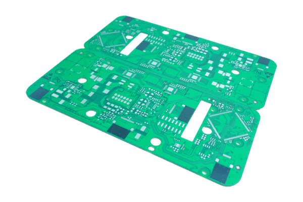
The antenna should be prioritized to be placed at the edge of the PCB, away from metal components and structural parts (distance ≥ 3mm), and avoid wiring or copper laying below. In multi-layer board design, the top radiation layer and the bottom ground plane need to be shielded from interference through a via array, and the middle signal layer can be partially hollowed out to improve efficiency (the case shows that the efficiency can be increased from 42% to 68%). The Bluetooth antenna feed point should be close to the IC, and the wiring should be straight or smooth to reduce impedance transients.
3. Impedance matching and simulation verification
The input impedance of the antenna needs to be matched with the RF circuit (usually 50 Ω), and the return loss (≥ 10dB) and bandwidth (such as covering 200MHz in the 2.4GHz frequency band) should be optimized through simulation software (such as HFSS, CST). During debugging, a 2-7mm length margin can be reserved to adapt to actual environmental changes.
2、 Key precautions

1. Environmental interference avoidance
The antenna area should be kept away from metal components such as motors and speakers to avoid conductive spraying or electroplating processes. If the shell is made of metal material, plastic windows or non-conductive coatings should be used. The distance between the built-in antenna and the battery should be ≥ 5mm to prevent electromagnetic shielding.
2. Integrity of high-frequency signals
RF wiring must strictly follow 50 Ω impedance control, avoiding via holes and right angle corners (recommended>90 °). When wiring with dual panels, the wires on both sides should be crossed or bent to reduce parasitic coupling. Wiring is prohibited below the amplifier IC and must be grounded through a via array for heat dissipation.
3. Thermal management and material adaptation in PCB antenna design
High frequency signals can easily cause local heating, and thermal conductive silicone columns or heat dissipation through holes need to be arranged in the RF area. FR4 board has low cost but high high-frequency loss. For millimeter wave scenarios, it is recommended to use a mixed dielectric substrate (such as Rogers material laminated with FR4) to balance performance and cost.
3、 Typical Applications and Trends
MIFA (Twisted Line Antenna) is widely used in smart homes and wearable devices due to its small footprint (7.2mm × 11.1mm) and wide bandwidth (150-250MHz). In the future, with the popularization of WiFi6E and UWB technologies, multi band coupled antennas (such as tri band slotted designs) and AI assisted optimization (such as deep learning iterative structures) will become mainstream directions.
Overall, PCB antenna design is a fusion of electromagnetics, materials science, and engineering experience, requiring a balance between miniaturization and high performance. Only through scientific simulation verification and rigorous process control can stable wireless communication performance be achieved between square inches.