The double-sided BGA (Ball Grid Array) design not only improves the integration of circuit boards, but also increases the complexity of layout, signal integrity, heat dissipation, and process implementation. The following are key considerations in double-sided BGA design, covering multiple dimensions such as layout, electrical, process, and reliability:
Table of Contents
1、 Component Layout and Mechanical Design
1. High conflict avoidance
-To avoid overlapping BGA components or other high components (such as electrolytic capacitors and heat sinks) on both sides in the vertical direction, it is necessary to plan the height of the components in advance and reserve sufficient space (usually it is recommended to have a component spacing of ≥ 2mm, and increase the spacing when the height difference is large).
-Prioritize placing large BGAs (such as processors and FPGAs) on the same side, and layout small BGAs or low height components on the other side to reduce stacking risks.
2. Heat dissipation planning
-BGA components with high heat generation should be dispersed on different surfaces as much as possible to avoid heat concentration. Heat dissipation copper foil, thermal via, or embedded heat pipe/heat spreader can be designed below the component.
-If a heat sink needs to be installed on the backside BGA component, space should be reserved in advance and sufficient mechanical strength of the circuit board should be ensured (such as increasing substrate thickness or using metal core PCB).
3. Layout symmetry and process compatibility
-The double-sided BGA layout needs to consider the SMT placement sequence (usually soldering one side of the large component first, and then soldering the other side) to avoid the influence of high temperature on the already soldered components during soldering.
-The layout of components should be as symmetrical as possible to reduce thermal deformation of the circuit board; Simultaneously reserve process edges (≥ 5mm) and positioning holes for precise alignment of the surface mount machine.
2、 Signal integrity and power supply design
1. Layered structure and via management
-Adopt a reasonable stacking scheme (such as adding power layers and geological layers), and control impedance matching (such as differential signals and high-speed buses). Double sided BGA may require more via cross layers, and the via density needs to be optimized to avoid substrate cracking caused by “via forest”.
-High speed signals (such as DDR, PCIe) should be routed through the inner layer as much as possible to reduce the path length difference and delay deviation caused by double-sided wiring. Avoid key signals crossing segmentation areas (such as power/ground plane fractures).
2. Power and ground network design
-Assign independent power layers to double-sided BGA and connect the power pads on both sides through multiple vias to reduce impedance.
-Decoupling capacitors (especially high-frequency capacitors) should be placed near the BGA power pins, preferably on the same side of the component, to reduce parasitic inductance introduced by cross layer vias. If cross layer is required, the path from the capacitor to the pin needs to be shortened.
3. Interference and EMC control
-When wiring on both sides, avoid parallel routing of high-speed signals on both sides (especially sensitive signals such as clock and RF lines), and reduce crosstalk through layer isolation or orthogonal wiring.
-The formation around BGA needs to be intact, with reserved positions for electrostatic discharge (ESD) devices such as TVS tubes and magnetic beads.
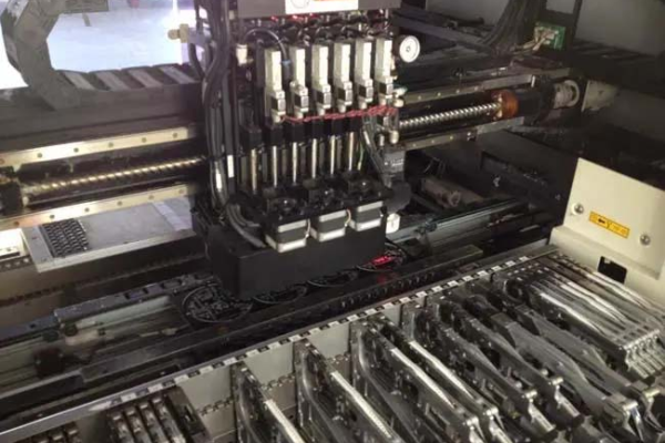
3、 Welding Process and Manufacturability (DFM)
1. Welding sequence and temperature curve
-Prioritize soldering larger or heat-resistant BGA (such as ceramic packaging) on the bottom layer, and then soldering the top layer components. Reflow soldering should use a “stepped” temperature curve to avoid the impact of secondary soldering on the underlying components (such as solder ball melting causing displacement).
-Confirm the reflow soldering capability of the PCB manufacturer (such as maximum temperature and number of temperature zones) to avoid carbonization or delamination of the substrate due to multiple high-temperature baking.
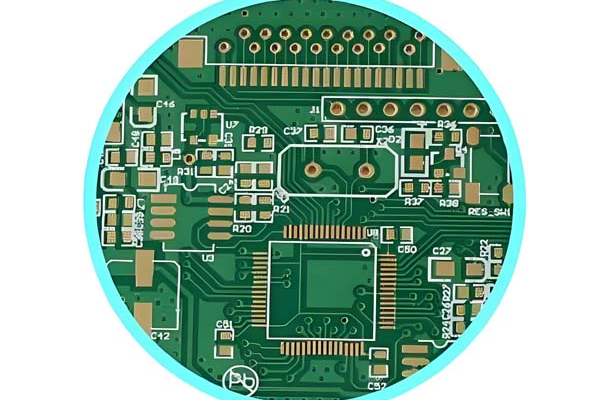
2. Pad and solder mask design
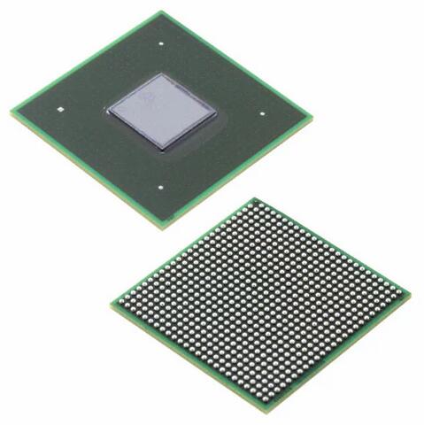
-The size of BGA solder pads must strictly follow the manufacturer’s specifications, and solder mask openings can be designed with “Non Solder Mask Defined” (NSMD) or “Positive Chip” (SMD). NSMD can reduce solder pad stress, but attention should be paid to solder pad spacing to avoid bridging.
-The solder pads of the backside BGA should avoid conflicts with the through holes of the front-end components, especially in buried/blind hole designs, ensuring that the through holes are not located directly below the solder balls (which may cause solder holes).
3. Solder ball spacing and component tolerance
-For fine pitch BGA (such as ≤ 0.5mm), it is necessary to evaluate the SMT accuracy of the assembly plant (such as SMT machine resolution, SPI/AOI detection capability) to avoid solder ball offset or short circuit caused by alignment deviation.
-Reserve repair space during component layout to facilitate independent disassembly of damaged single-sided BGA components without affecting the other side components.
4、 Reliability and mechanical strength
1. Substrate material and thickness
-Select high Tg (≥ 170 ℃) and low CTE (coefficient of thermal expansion) plates (such as FR-4 TG170, Rogers high-frequency plate) to reduce stress cracking under thermal cycling. For double-sided BGA, it is recommended to have a substrate thickness of ≥ 1.6mm or increase the number of glass fiber layers to enhance rigidity.
2. Stress release and support design
-To avoid large areas of copper foil voids around BGA, stress can be dispersed through grid shaped copper foil or heat dissipation vias. If the component size is large (such as ≥ 25mm × 25mm), metal supports (such as steel sheets) can be added to the back of the substrate or embedded design can be adopted.
-Avoid arranging dense vias, especially through holes, directly below the BGA to prevent copper filling in the vias from breaking and causing electrical connection failure.
3. Moisture prevention and protection
-The double-sided BGA area should avoid exposing the substrate to humid environments, and can be treated with immersion gold (ENIG) or OSP surface treatment, and coated with anti moisture, anti mold, and anti salt spray paint after assembly.
5、 Testing and Debugging
1. Test point reservation
-The pins of double-sided BGA are usually covered by solder balls, making it difficult to test directly. It is necessary to reserve test points on the critical signal path (such as pile driving holes, surface test pads) and ensure that the test points are not obstructed by the components on the other side.
-Adopting boundary scan (JTAG) or built-in self-test (BIST) functionality to reduce reliance on physical test points.
2. Repackable design
-The repair of BGA on the back requires higher temperatures, which may cause the front components to detach. Therefore, it is necessary to evaluate the temperature resistance level of the components (such as maximum reflow temperature ≤ 260 ℃), or adopt a staged soldering process (such as soldering high-temperature components first, and then soldering low-temperature components).
6、 Design collaboration and review
-Communicate with the manufacturer in advance: confirm the number of PCB layers, minimum line width/spacing, via type (such as blind hole/buried hole cost), component pad compatibility, etc.
-Multi round DFM/DFA review: Check spacing, stacking, heat dissipation, etc. through simulation tools such as Altium and Cadence to avoid design defects.
-Sample verification: After the first piece is produced, X-ray inspection (checking the void rate of solder balls) and ICT/FCT testing are conducted to verify electrical performance and mechanical reliability.
Summarize
The design of double-sided BGA requires a balance between integration, performance, and process, with the core being layout rationalization, signal integrity optimization, heat dissipation and mechanical strength assurance, and process compatibility matching. By planning ahead and following design specifications, risks can be effectively reduced, and product yield and reliability can be improved.
Get your exclusive quote immediately: fill out the form or send an email directly.As a professional PCB manufacturer for hobbyist , we will provide you with a quote service within 24 hours. Enjoy free DFM optimization and a 10% discount on SMT patches for your first order!