The quality of PCBA (Printed Circuit Board Assembly) directly affects the reliability, lifespan, and performance of electronic products. Its quality control needs to run through the entire process of design, materials, production, testing, environment, etc. The core is “prevention first, process control as a supplement, and post traceability as a backup”. The following are key measures to ensure PCBA quality in production:
Table of Contents
Ⅰ. Source Control: Design and Material Quality
1. Implementation of Design for Manufacturability (DFM/DFA)
During the design phase, it is necessary to avoid production hazards in advance and reduce quality problems caused by unreasonable design
-DFM (manufacturability): Clearly define the minimum line width/spacing, via size, and pad size (in accordance with IPC standards such as IPC-A-610) to avoid solder interference caused by the layout of fine pitch components (such as 0.4mm BGA) being too close to large-sized components (such as connectors);
-DFA (Assemblability): The pin length of the plug-in components should be uniform (it is recommended to extend the solder pad by 1.5-2mm) to avoid bridging caused by excessive length or virtual soldering caused by insufficient length; The solder pad design of surface mount components (SMD) matches the component packaging (such as the width of the solder pads for resistors and capacitors being 1.1-1.2 times the size of the component) to prevent defects such as “monument” and “offset”.

-Confirm the process capability (such as SMT equipment accuracy and reflow oven temperature range) with the production plant in advance to ensure that the design parameters are within the controllable range of the production equipment.
2. Quality control of electronic components
Poor quality materials cannot produce high-quality PCBA. It is necessary to strictly control the procurement and inspection of electronic components
-Supplier management: Select qualified original factories or authorized agents, establish a supplier grading system (A/B/C levels), and conduct regular audits (such as ISO9001 certification and quality traceability);
-Incoming Quality Control (IQC):
-Appearance: Check for oxidation, deformation, and damage of component pins, clarity of silk screen printing, and anti-static packaging (ESD sensitive components must have anti-static labels);
-Performance: Key components such as ICs, capacitors, and crystal oscillators need to be sampled and tested (using LCR meters to measure capacitance values and oscilloscopes to measure crystal oscillator frequencies) to ensure that the parameters comply with the specifications;
-Batch traceability: Record the component batch number and production date, bind them with the PCBA production batch, and facilitate subsequent traceability.
-Storage and turnover: ESD sensitive components such as ICs and MOS tubes should be stored in anti-static packaging (anti-static bags, moisture-proof cabinets), and humidity sensitive components (MSD, such as BGA) should be baked according to the humidity card instructions (such as 85 ℃/24 hours) to avoid moisture absorption and “popcorn” phenomenon during welding.
Ⅱ.Core production process: SMT and THT process control
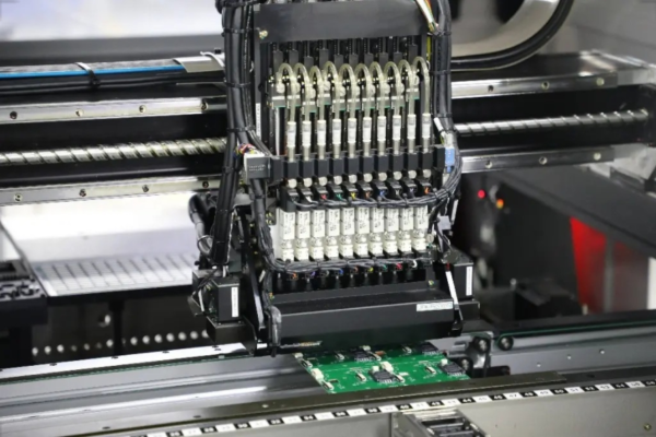
1. Key control points of SMT (Surface Mount Technology)
SMT is a critical area for PCBA quality, requiring a focus on three major steps: solder paste printing, component mounting, and reflow soldering
-Solder paste printing:

-Steel mesh design: The opening size matches the solder pad (such as 0402 component steel mesh opening is 5% -10% smaller than the solder pad to prevent solder paste overflow), and the thickness is selected according to the size of the component (0.12-0.15mm, 0.1mm for fine pitch components);
-Printing parameters: scraper pressure (5-10N), speed (20-50mm/s), and demolding speed (1-3mm/s) need to be adjusted to the optimal state to ensure uniform solder paste volume (without less solder, more solder, or offset);
-Solder paste management: Low temperature storage (2-10 ℃), with a temperature recovery of more than 4 hours (to avoid condensation of water vapor), stirred evenly during use (to prevent component separation), and scrapped if not used up after 24 hours.
-Component mounting:
-Equipment calibration: Regularly verify the accuracy of the suction nozzle and positioning camera of the surface mount machine (ensuring an error of ± 0.01mm) to prevent component misalignment and wrong parts;
-Selection of suction nozzle: Match according to the size of the component (such as using a 0.3mm suction nozzle for 0201 component and a dedicated suction nozzle for BGA), to avoid nozzle wear and component detachment;
-Process parameters: mounting pressure (0.1-0.5N, smaller pressure for small components), speed (50-100mm/s), to prevent excessive pressure from damaging components (such as ceramic capacitors) or insufficient pressure from causing virtual mounting.
-Reflow soldering:
-Temperature curve: Set preheating zone (150-180 ℃, remove flux volatiles), constant temperature zone (180-210 ℃, activate flux), reflow zone (peak 230-250 ℃, time 30-60s), and cooling zone (≤ 100 ℃/s cooling) according to the type of solder paste (such as Sn63Pb37 melting point 183 ℃, SAC305 melting point 217 ℃), to avoid component oxidation or PCB discoloration caused by high temperature, and cold soldering caused by low temperature;
-Nitrogen protection inside the furnace: For fine pitch components (such as 0.4mm BGA) or products with high reliability requirements, nitrogen gas (oxygen content ≤ 500ppm) is filled to reduce solder oxidation and improve solder joint glossiness.
2. Key control points of THT (through-hole insertion technology)
For plug-in components such as connectors and electrolytic capacitors, it is necessary to control the correctness of the plug-in and the wave soldering process:
-Plug in inspection: Ensure that the pins are inserted correctly into the solder pads (without any incorrect or missing connections), and that the pin extension length meets the requirements (1-2mm above the solder pads and 0.8-1.5mm below);
-Wave soldering parameters: uniform flux spraying (covering all solder joints), preheating temperature (100-120 ℃), peak temperature (250-260 ℃, SnPb solder) or 260-270 ℃ (lead-free solder), chain speed (1.2-1.8m/min), to prevent bridging (excessive tin) and solder leakage (insufficient flux);
-Cutting process: After inserting, the cutting length of the legs should be uniform (0.8-1.2mm) to avoid short circuits caused by too long or insufficient welding strength caused by too short.
Ⅲ.Full process inspection: timely detection of defects
Testing is not the goal, but to prevent the outflow of defective products. It is necessary to establish a multi-level testing system:
1. Online detection (during the process):
-AOI (Automatic Optical Inspection): After SMT (mounting, reflow soldering), inspect the appearance of solder joints (virtual soldering, bridging, misalignment, wrong parts, missing parts) with an accuracy of up to 0.01mm, replacing the fatigue error of manual visual inspection;
-SPI (Solder Paste Inspection): After printing, detect the amount, area, and offset of solder paste, adjust printing parameters in a timely manner, and reduce subsequent welding defects;
-AXI (Automatic X-ray Inspection): For “bottom solder joints” (invisible solder joints) such as BGA, CSP, QFN, etc., detect solder ball voids (void rate ≤ 25% is qualified) and virtual soldering to avoid hidden defects.
2. Offline detection (after finished product):
-ICT (Online Testing): By using needle bed contact test points, detect circuit connectivity (open circuit, short circuit), component parameters (resistance, capacitance, diode forward voltage drop), and eliminate faulty or damaged components;
-FCT (Functional Testing): Simulate the actual working environment of the product, test key functions (such as voltage output, signal transmission, communication protocol), and verify whether the PCBA meets design specifications;
-Manual re inspection: Conduct manual visual inspection on areas that cannot be covered by AOI/AXI, such as connector pins and large-sized component solder joints, with a focus on checking the solder fullness and absence of burrs.
3. Reliability testing (sampling):
-For high reliability products (such as automotive electronics and industrial equipment), sample for environmental tests: high and low temperature cycles (-40 ℃~85 ℃, 100 cycles), vibration tests (10-2000Hz, 10g acceleration), and damp heat tests (40 ℃/90% RH, 1000 hours) to verify the anti-aging ability of solder joints and components.
Ⅳ. Process Management: Standardization and Traceability
1. Standardized Operating Procedures (SOP):
Develop detailed SOPs for each process (such as solder paste printing steps, SMT machine operation procedures, testing standards), clarify operating points (such as “daily testing of resistance values 1-35M Ω for anti-static wristbands”), and train and assess operators to ensure consistency in execution.
2. Equipment maintenance and calibration:

-SMT equipment: The suction nozzle of the SMT machine is cleaned daily, and the track is lubricated weekly; Monthly calibration of temperature sensors for reflow soldering furnaces (using thermocouples to verify that the actual furnace temperature deviates from the set value by ≤ 3 ℃);
-Testing equipment: AOI calibrates the optical system weekly, and ICT needle beds clean the probes monthly to prevent poor contact.
3. Quality traceability system:
-Record key data: production batch, component batch, equipment number, operator, testing results, and form a “production resume”;
-Using QR code/barcode: Each PCBA is bound with a unique identifier, and scanning the code can trace the entire process information, making it easy to analyze the cause of defective products.
Ⅴ.Environment and Personnel: Basic Support
1. Production environment control:
-Temperature and humidity: SMT workshop temperature is 20-26 ℃, humidity is 40% -60% (to prevent solder paste from absorbing moisture and static electricity accumulation);
-Cleanliness: SMT workshop ≥ Class 10000 (≥ 0.5 μ m particles ≤ 10000 per cubic foot), to avoid dust causing solder joint virtual soldering;
-ESD protection: Ground, workbench, equipment grounding (grounding resistance ≤ 4 Ω), operators wear anti-static wristbands/shoes, and turnover materials (material boxes, trays) are made of anti-static materials.
2. Personnel management:
-Training: New employees must complete training on SMT technology, ESD protection, testing standards, etc., and pass the assessment before they can take up their positions;
-Quality awareness: Strengthen employees’ sense of responsibility and encourage proactive problem discovery through “sharing of defective product cases” and “quality reward and punishment system” (such as the “self inspection and mutual inspection” system).
Summarize
The core of PCBA quality control is “full process prevention+key link control+closed-loop traceability”. By optimizing design to reduce production difficulty, ensuring source quality through material inspection, controlling process defects through standardized production and precise detection, and ultimately combining environmental and personnel management, we achieve “low-cost, high reliability” PCBA mass production. At the same time, it is necessary to establish a continuous improvement mechanism (such as weekly quality analysis meetings, using Plato to analyze the defects with the highest defect rate and optimize them accordingly) to continuously improve quality stability.
Get your exclusive quote immediately: fill out the form or send an email directly, and we will provide you with a quote service within 24 hours. Enjoy free DFM optimization and a 10% discount on SMT patches for your first order!