The Ultimate Guide to HDMI Interface PCB Design: Signal Integrity, EMI Protection, and High Speed Cabling Practices
Today, with the popularity of 4K/8K video and VR devices, the transmission rate of HDMI 2.1 interface has reached 48Gbps, posing extreme challenges to PCB design. Data shows that 90% of HDMI signal failures are caused by impedance mismatch, EMI interference, and layout errors. This article will delve into the five core design principles to help you achieve zero defect HDMI interfaces.
Table of Contents
1、 Signal integrity design: eliminating reflections and crosstalk
1. Topology optimization of transmission lines
-Shortest path principle: The distance between the HDMI connector and the driver IC should be ≤ 50mm to reduce signal attenuation
-Differential pair internal equal length: internal length deviation ≤ 5mil (such as clock differential pair D ± CLK)
-Equal length between differential pairs: The length deviation of four sets of differential pairs (CLK+3 × Data) is ≤ 10 mil
2. Crosstalk suppression technology
-3W spacing rule: Differential line spacing ≥ 3 times line width (e.g. 30mil spacing is required for a 10mil line width)
-Ground wrapping treatment: The ground wire is laid on both sides along the differential line, with ground holes (diameter 8mil/16mil) drilled at intervals of 100mil
-Cross layer isolation: Orthogonal layout of adjacent signal layer routing to reduce capacitive coupling
2、 Impedance matching: 100 Ω differential impedance precise control
Stacking and Line Width Specifications
| Parameters | HDMI 1.4/2.0 (≤ 18Gbps) | HDMI 2.1 (48Gbps) |
| Differential impedance | 100 Ω± 10% | 100 Ω± 5% |
| Line width/spacing | 10mil/6mil | 8mil/5mil |
| Reference plane | Complete GND layer | Dual GND layer clamping |
| Via size | 8mil/16mil | Laser micro hole 6mil/10mil |
Key formula:
Calculation of microstrip line impedance:
| Z₀ = 87/√(εᵣ+1.41) × ln(5.98H/(0.8W+T)) |
(H: dielectric thickness, W: line width, T: copper thickness)
Through hole optimization:
-Backdrill residual stub ≤ 10mil (for signals ≥ 5Gbps)
-Place 2 grounding vias next to each signal via
3、 EMI protection design: three-level electrostatic defense system
1. Device selection and layout
-ESD protection chip: selection based on IEC 61000-4-2 Level 4 (contact discharge 30kV)
-Common mode inductance: impedance ≥ 100 Ω @ 100MHz, placed in the rear stage of ESD devices
-Spacing rule: ESD devices should be 1.5mm away from HDMI terminals (thickness of soldering iron tip) to avoid soldering
2. Shielding architecture design
-Connector shielding shell: connected to the metal shell through spring pins, with a grounding impedance of<10m Ω
-GND isolation slot: dig 1mm non-metallic slot between high voltage area (5V power supply) and signal area
4、 Layout and wiring rules: Key points for high-density HDI practical use
1. Layout Iron Law

-The HDMI connector is placed at the edge of the board, extending ≥ 2mm outside the board for easy insertion and removal
-5V power supply circuit distance from interface ≤ 15mm, using 2oz copper foil+15ml line width
-Impedance matching resistors are placed side by side (not front to back arrangement) to avoid residual pile effects
2. Wiring exclusion zone
-Prohibit right angle turns: Use 45 ° curved or angled wiring to reduce RF radiation
-Prohibition of cross segmentation: Maintain a complete reference plane below the differential line, and connect a 0.1 μ F capacitor across the gap
-High speed signal layer: Avoid changing layers by routing the TOP layer, and add accompanying ground holes when changing layers is necessary
5、 Testing and Verification: Dual Insurance of Simulation and Actual Testing
1. Pre production simulation
-Channel modeling: Extracting S-parameter models for connectors/cables/PCBs
-Eye diagram test: 48Gbps signal requires eye width>0.3UI and eye height>80mV
2. Physical layer testing items
| Test items | Standard tools | Qualification indicators |
| Impedance consistency | TDR measuring instrument | Δ Z ≤± 5% |
| Differential latency difference | High speed oscilloscope | ≤ 5ps |
| ESD immunity | Electrostatic gun simulator | Discharge through ± 15kV |
| Return loss | Vector network analyzer | > 15dB@24GHz |
3. Mass production monitoring:
-AOI detection of differential line notches/burrs (resolution ≤ 10 μ m)
-100% flying pin test for short circuit/open circuit
Future trend: 48Gbps+design preparation plan
1. Material upgrade:
Using Megtron 6 (Df=0.002) or Rogers 4350B (Df=0.0037) substrate
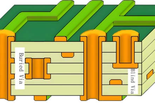
2. Any layer HDI:
Laser blind hole stacking (1+N+1) achieves<50 μ m micropores
3. AI Anti Interference Algorithm:
Real time optimization of wiring paths, reducing crosstalk by 40%
→ [Download HDMI 2.1 Design Checklist]
Includes impedance calculation template, ESD layout specification, and simulation parameter set