In the rapid development of 5G communication, new energy vehicles, and AI servers, PCB thermal management has become a core factor determining equipment reliability and performance. This article provides a comprehensive analysis of the entire process solution for PCB thermal management, from heat dissipation technology and material innovation to industry applications, to help enterprises overcome heat dissipation bottlenecks in high-power density scenarios.
1、 Three major risks and response strategies of thermal management failure
1. Performance degradation: For every 10 ℃ increase in temperature, the lifespan of electrolytic capacitors is reduced by 50%. It is necessary to reduce thermal resistance through the design of inner copper plane heat dissipation and thermal through-hole array.

2. Mechanical deformation: Multilayer PCBs are prone to warping due to differences in material thermal expansion coefficients. Ceramic substrates (thermal conductivity ≥ 170W/m · K) can be used to achieve a thermal expansion matching degree of 99.7%.
3. Signal interference: High temperature causes impedance deviation of ± 15%, and thermal simulation tools need to be used to optimize the copper thickness (recommended ≥ 2oz) and heat dissipation path.
2、 The Five Core Technologies of PCB Thermal Management
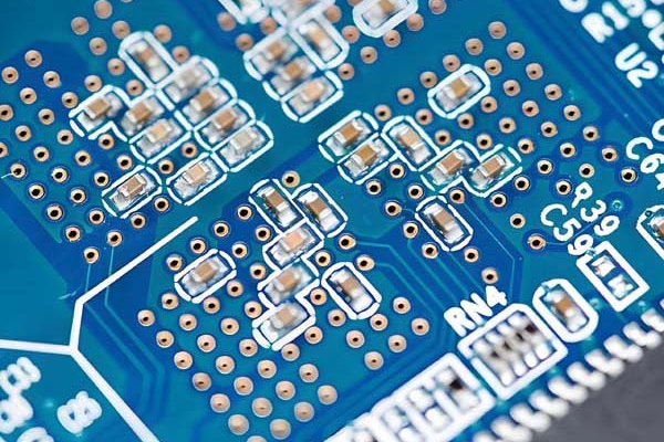
1. Stacked heat dissipation architecture
-The four layer board adopts a “signal ground power signal” stacking method, which forms electromagnetic shielding through dual ground planes and reduces power noise by 40%.
-The six layer board recommends the “TOP-GND Signal PWR-GND-BOTTOM” structure, which utilizes vertical thermal conduction channels to reduce thermal resistance by 0.35 ℃/W.
2. Innovation in Materials and Processes
-Ceramic substrate: Aluminum nitride ceramic copper-clad laminate (DBC) has a 60% increase in thermal conductivity compared to traditional FR-4, and is suitable for extreme environments ranging from -40 ℃ to 125 ℃.
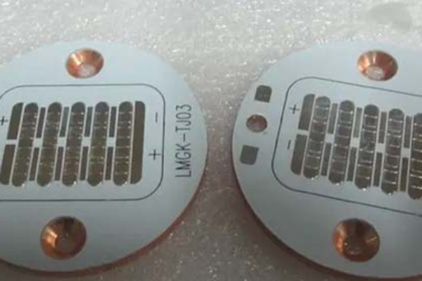
-Copper paste plug hole: Jialichuang’s “copper paste disk hole” process fills the hole with high thermal conductivity copper paste (8W/mK), increasing the heat dissipation contact area by 300%.

3. Thermal path optimization design
-Arrange a heat dissipation via matrix (≥ 10 per square centimeter) below the heating element, and connect each layer of copper foil through electroplated copper, reducing the junction temperature by 15 ℃.
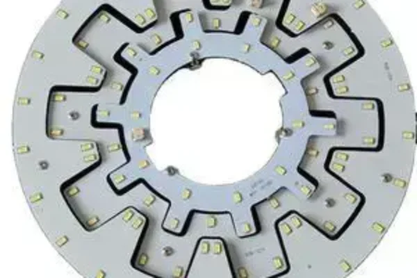
-Adopting a stepped “copper coin” structure, the heat dissipation area is increased by 55 times, making it suitable for micro devices and extreme space environments.
4. Intelligent cooling system
-Integrating temperature sensors and AI control modules, dynamically optimizing heat dissipation paths, and improving system energy efficiency by 15%.
-CFD simulation verifies the heat dissipation scheme, with a predicted hotspot distribution error of ≤ 2 ℃.

5. Industry customized solutions
-New energy vehicles: High temperature resistant copper substrate+liquid cooled flow channel design, IGBT module peak temperature reduced from 135 ℃ to 98 ℃.
-5G base station: Metal ceramic composite structure can withstand high humidity environments, with a high temperature derating rate of ≤ 5%.
If you need customized heat dissipation solutions, please feel free to contact our engineering team!