In today’s hyper-connected world, your electronic device doesn’t operate in a vacuum. It must function flawlessly amidst a cacophony of electromagnetic noise while also ensuring it doesn’t become a source of interference itself. This dual challenge is Electromagnetic Compatibility (EMC).
Fail EMC testing, and you face costly redesigns, delayed product launches, and compliance barriers. The most effective, and often most overlooked, weapon in achieving EMC isn’t a shielding can or a ferrite bead—it’s the Printed Circuit Board (PCB) design itself.
Up to 80% of EMC performance is determined by choices made during the PCB layout phase. This article explores the critical PCB design principles that separate EMC-compliant products from problematic ones.
Table of Contents
The Foundation: Understanding EMI Coupling Paths
Electromagnetic Interference (EMI) travels via three primary paths, and your PCB design must address all of them:
1.Conductive Coupling: Noise traveling through physical conductors (traces, power planes, cables).
2.Radiated Coupling: Noise propagating through the air as electromagnetic fields from traces or components.
3.Common-Impedance Coupling: Noise shared between circuits through a common path, like a shared ground return.
A robust PCB design systematically blocks these paths at the source.
Core PCB Design Strategies for Superior EMC
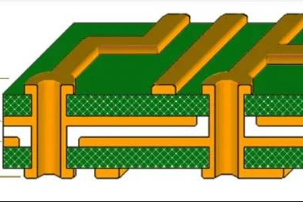
1. The Strategic Stack-Up: Your Blueprint for Success
Your layer stack-up is the most critical EMC decision. A poorly planned stack-up is a losing battle.
•The Power of Image Planes: Always route high-speed signals adjacent to a continuous solid reference plane (power or ground). This provides a low-inductance return path, containing the electromagnetic fields and drastically reducing radiation.
•The “Capacitor in the Middle” Trick: For complex boards, use symmetrical, tightly coupled stack-ups. Placing signal layers between two plane layers creates inherent, distributed capacitance that decouples high-frequency noise.
Recommended 4-Layer Stack-Up:
| Layer | Function | EMC Benefit |
| L1 | Signal (High-Speed) | Top layer for sensitive components |
| L2 | Ground Plane (Solid) | Provides return path for L1 signals |
| L3 | Power Plane | Distributes clean power |
| L4 | Signal (Low-Speed) | Bottom layer for slower, less critical routing |
For advanced designs (8-Layers+), dedicate entire layers to ground, creating a “shielded” environment for sensitive signals.
2. Grounding: The Art of Controlling Return Currents
There is no “one perfect grounding strategy,” but the goal is always the same: control the return current path.
•Avoid “Ground Loops”: These act as efficient loop antennas. Use a solid ground plane whenever possible.
•Partitioning (But Carefully): Split grounds only when necessary (e.g., separating analog and digital grounds) and join them at a single point, typically under the ADC or where the power enters the board. Improper splitting is worse than no splitting at all.
•Star Grounding for Power: Bring all power returns to a single point to prevent common-impedance coupling between different circuits.
3. Routing: Where the Battle is Won or Lost
•The 3-W Rule: Keep sensitive traces (especially clocks) at least 3 times the trace width (3W) away from other traces to minimize crosstalk.
•Minimize Loop Areas: This is the Golden Rule of EMC. The larger the loop area formed by a signal and its return current path, the more efficient it is at radiating energy. Keep high-speed traces and their return paths as close as possible.
•Avoid 90-Degree Corners: Use 45-degree angles or rounded corners. 90-degree corners increase capacitance at the corner, causing reflections and acting as point radiators.
•Differential Pair Routing: For high-speed interfaces (USB, HDMI, PCIe), route differential pairs with consistent spacing and exactly matched lengths (length tuning).
4. Power Integrity: The Bedrock of EMC
A noisy power supply is a broadcast antenna on your PCB.
•Strategic Decoupling: Use a combination of bulk capacitors (10uF-100uF), ceramic capacitors (0.1uF), and small-value high-frequency capacitors (0.01uF) placed as close as possible to the power pins of ICs. Each handles a different frequency range of noise.
•Power Plane Islands: For very noisy circuits (e.g., a switching regulator), create a dedicated power island using a ferrite bead or a 0Ω resistor to filter noise before it contaminates the main power plane.
5. Component Placement & Shielding
•Zoning: Group components by function (e.g., power supply, analog, digital, RF). This prevents noisy circuits from interfering with sensitive ones and allows for targeted shielding.
•Shielding Cans: Plan for them early. Provide a generous, well-staked (with many vias) grounding pad on the PCB for any shielding can to ensure a low-impedance connection to the ground plane.
Common EMC Problems and Their PCB Design Fixes
| EMC Failure Symptom | Likely PCB Design Cause | Solution |
| Radiated Emissions | Large loop areas in high-speed clocks/data lines. | Route clocks first, keep them short, and adjacent to a solid ground plane. Use guard traces with grounding vias. |
| Power Supply Noise | Inadequate decoupling or poor power plane design. | Add high-frequency decoupling caps closer to ICs. Use a power plane instead of power traces for noisy circuits. |
| Susceptibility to ESD | Long traces acting as antennas, poor grounding on connectors. | Add TVS diodes at I/O connectors. Ensure a low-impedance path from connector ground to chassis ground. |
| Crosstalk | Traces routed too close and parallel for too long. | Enforce the 3W rule. Route traces on different layers perpendicular to each other to minimize overlap. |
How SysPCB Engineers EMC Success from the Ground Up
Achieving EMC is not about magic; it’s about methodical application of physics and best practices. At SysPCB, we don’t just manufacture your boards—we partner with you to ensure they are designed for success.
Our EMC-Optimized Capabilities Include:
•DFM/DFA with an EMC Focus: Our engineering review identifies potential EMC pitfalls in your design before it goes to production.
•Advanced Materials: We work with a range of low-loss, controlled-Dk laminates (Rogers, Isola, Megtron) ideal for high-speed, low-noise designs.
•Precision Manufacturing: Tight impedance control (±5% or better), accurate layer-to-layer registration, and superior plating ensure your carefully designed stack-up and traces perform as intended.
•Any-Layer HDI & Microvias: These technologies allow for incredibly dense routing while maintaining excellent signal integrity and minimizing loop areas.
Let us help you design silence into your next product.
Your PCB is the foundation of your product’s EMC performance. A well-designed board reduces the need for external fixes, saves cost, and gets you to market faster with a more reliable product.
Explore our advanced PCB manufacturing capabilities that bring your EMC-critical designs to life: