From sunlight to socket: the critical role of precision-engineered PCBs in harnessing solar energy efficiently.
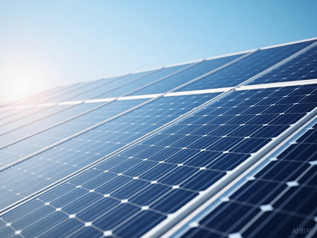
The global transition to renewable energy is accelerating, with solar power leading the charge. At the heart of every solar energy system lies a critical component: the solar inverter—and its performance hinges on the printed circuit board (PCB) that powers it. As solar technology evolves toward higher efficiencies, greater reliability, and broader applications, PCB design and manufacturing have become fundamental to unlocking the full potential of solar energy conversion. From rooftop installations to vast solar farms, advanced PCBs enable the sophisticated power electronics that make modern solar energy possible.
Table of Contents
The Solar Inverter Landscape: More Than Just Conversion
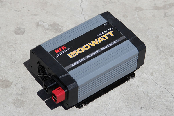
Solar inverters perform the essential function of converting the direct current (DC) output from solar panels into alternating current (AC) suitable for the grid or off-grid use. However, their role has expanded to include maximum power point tracking (MPPT) to optimize energy harvest, grid management functions, and system monitoring capabilities.
The performance demands on these systems are extreme:
– Conversion efficiencies now exceed 98.5% for leading designs
– Lifespans must reach 15+ years with minimal maintenance
– Operation in harsh environments from desert heat to alpine cold
– Compliance with strict safety and grid regulations worldwide
Meeting these challenges requires PCBs that go far beyond conventional designs, incorporating specialized materials, innovative thermal management, and precision engineering.
Critical PCB Technologies for Solar Inverters
Advanced Materials for Extreme Conditions
Solar inverters demand PCBs that can withstand thermal stress, environmental challenges, and electrical demands that far exceed consumer electronics requirements.
Thermal Management Materials are particularly crucial in solar applications. Inverters for high-altitude installations face unique thermal challenges due to decreased air density, which reduces natural convection cooling. Specialized solutions have emerged to address these constraints:
Table: Advanced PCB Materials for Solar Inverters
| Material Type | Key Properties | Benefits for Solar Inverters | Applications |
| Aluminum-based PCB | Excellent thermal conductivity (180-260 W/mK), mechanical strength | Efficient heat dissipation, high durability | High-power components, switching devices |
| Ceramic-filled PTFE | Low dielectric loss (Df ≤0.002), stable εr | Stable high-frequency performance | RF components, communication modules |
| High-Tg FR-4 | Glass transition temperature ≥170°C | Withstands temperature cycling, prevents delamination | Cost-sensitive designs |
| Thermal Clad Materials | Integrated thermal layers | Direct heat path from components | IGBTs, MOSFETs, diodes |
Insulation and Protection are equally critical, especially in high-altitude applications. One innovation involves “lines coated with an insulating protective layer” which significantly “improves the insulation strength of the inverter”. This enhanced insulation is vital for preventing arcing and short circuits in environments where low air pressure reduces dielectric strength.
Thermal Management: The Efficiency Frontier
Heat is the primary enemy of electronic reliability, and solar inverters generate substantial heat during operation. Effective thermal management is not merely desirable—it’s essential for long-term performance.
Innovative Cooling Solutions have emerged to address thermal challenges:
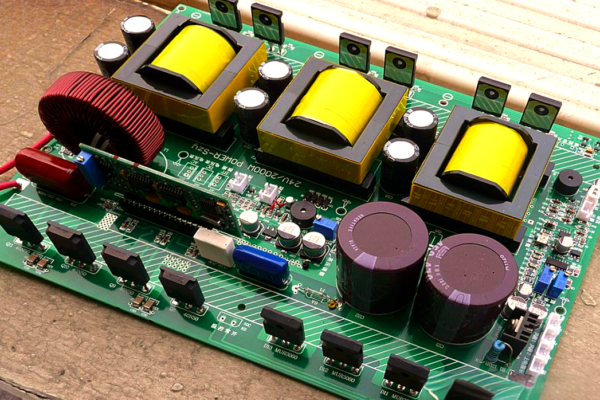
•Integrated Heat Pipe Systems: Some (plateau-type distributed photovoltaic grid-connected inverters) combine aluminum-based PCB with sophisticated heat pipe radiators (热管散热器). These systems feature “heat pipe evaporation ends, heat pipe condensation ends, and heat pipe transmission sections” that connect directly to “the aluminum-based metal layer and high-power components” for rapid heat transfer and dissipation.
•Strategic Component Layout: Proper placement of heat-generating components prevents thermal mutual heating and simplifies cooling architecture. This includes positioning MOSFETs away from other heat sources and ensuring adequate spacing for airflow.
•Copper Thermal Enhancements: Thick copper planes (2oz+), thermal vias under hot components, and embedded copper coins dramatically improve heat spreading. These approaches can “reduce device operating temperature by 15°C” and significantly extend system lifespan.
The implementation of advanced thermal management solutions directly impacts energy production. By maintaining optimal operating temperatures, these systems prevent efficiency degradation that typically occurs at elevated temperatures—a critical advantage in hot climate installations.
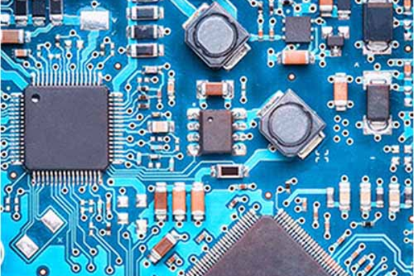
High-Density Interconnects for Power Electronics
Modern solar inverters pack increasing functionality into smaller form factors, demanding sophisticated PCB interconnection technologies.
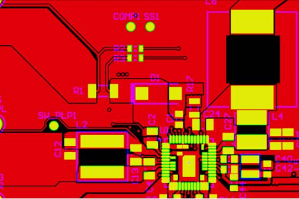
Any-Layer HDI and Microvias enable the complex routing required by dense component placement:
•Laser-drilled microvias (<0.1mm diameter) facilitate escape routing from fine-pitch BGAs used in digital control sections
•Stacked via configurations provide efficient vertical interconnection while managing thermal stresses
•Via-in-pad technology improves thermal and electrical performance of power components
These technologies enable inverters to achieve “20kHz switching frequency” while maintaining signal integrity and thermal performance.
Precision Impedance Control and Signal Integrity
As switching frequencies increase to reduce magnetic component size, maintaining signal integrity becomes increasingly challenging:
•Impedance-controlled routing (±5% tolerance) for gate drive signals prevents reflections and switching anomalies
•Differential pair routing for communication interfaces (CAN, RS485, Ethernet) ensures reliable system monitoring and control
•Guard rings and shielding protect sensitive analog measurement circuits from power switching noise
Specialized Solar Inverter Applications and PCB Solutions
Grid-Tied Inverters: Precision Meets Power
Grid-connected inverters require exceptional reliability and precise power quality management. Their PCBs must accommodate:
•High-power sections with adequate creepage and clearance distances
•Precision measurement circuits for voltage, current, and power quality monitoring
•Grid communication interfaces for data reporting and control commands
•Protection circuits that must respond within milliseconds to grid faults
The demanding nature of these systems is reflected in their certification requirements, with products needing to pass “TÜV IEC 62109 photovoltaic inverter safety certification” to meet “global major market access requirements”.
Microinverters and Power Optimizers: Density and Durability
Module-level power electronics present unique PCB challenges:
•Extreme miniaturization while maintaining isolation distances
•Outdoor operation directly behind solar panels, facing temperature extremes
•Decades of reliable operation with no maintenance
These applications often employ high-temperature laminates and conformal coatings to withstand the harsh environment behind solar panels, where temperatures can exceed 85°C.
Energy Storage Integration: The Future of Solar
As solar systems increasingly incorporate battery storage, inverters must manage bidirectional power flow:
•DC-DC converters for battery interface with wide voltage ranges
•Isolation barriers for safety in battery-connected circuits
•Enhanced monitoring for state-of-charge estimation and battery protection
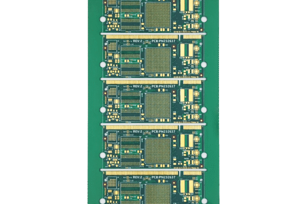
Manufacturing Excellence for Solar Applications
Precision Fabrication Processes
Solar inverter PCBs demand manufacturing capabilities beyond standard commercial boards:
•Controlled impedance fabrication with laser direct imaging for precise trace geometry
•Advanced plating processes for even copper distribution in high-current vias
•Optical inspection systems to verify solder mask coverage on high-voltage spacings
•Thermal stress testing to ensure reliability through temperature cycling
Quality Assurance and Long-Term Reliability
With expected service lives exceeding 15 years, solar inverter PCBs require rigorous quality management:
•Material traceability for critical high-reliability components
•Environmental testing including thermal cycling, humidity exposure, and vibration
•High-potential testing to verify isolation integrity
•Continuous process monitoring to minimize variation
The Future: Emerging Technologies in Solar Inverter PCBs
Wide Bandgap Semiconductors
Silicon Carbide (SiC) and Gallium Nitride (GaN) power devices are revolutionizing solar inverter design:
•Higher switching frequencies (50kHz+), reducing magnetic component size
•Higher temperature operation, reducing cooling requirements
•Improved efficiency, especially at partial load conditions
These advancements introduce new PCB requirements:
– Lower parasitic inductance layouts to manage increased dv/dt
– Enhanced thermal management for higher power density
– EMI mitigation strategies for higher frequency operation
Integrated Monitoring and Communications
Future solar inverters will incorporate increasingly sophisticated monitoring capabilities:
•Arc fault detection circuits with high sensitivity
•Grid impedance measurement for advanced grid support functions
•Wireless connectivity for maintenance and monitoring
Sustainability in PCB Manufacturing
As part of the renewable energy ecosystem, solar inverter PCBs are increasingly focused on sustainable manufacturing:
•Halogen-free materials and reduced hazardous substances
•Water-saving processes in fabrication
•Recycling and recovery of manufacturing materials
Conclusion: Engineering the Solar Future
The solar energy revolution depends fundamentally on the continued advancement of PCB technologies for power conversion. From material science innovations to precision manufacturing processes, each improvement in PCB capability enables more efficient, reliable, and cost-effective solar energy harvesting.
At SysPCB, we specialize in the advanced PCB technologies that power the solar industry:
– High-reliability designs for 15+ year service life
– Advanced thermal management solutions for demanding environments
– Precision manufacturing for high-voltage and high-current applications
– Comprehensive testing to ensure performance in solar applications
Our expertise in aluminum-based PCBs, thermal management strategies, and high-density interconnects has already enabled customers to achieve 98.5% conversion efficiency and 15-year operational lifespans—even in challenging environments like desert solar farms where temperatures reach 60°C.
Ready to power the solar energy revolution with your next inverter design?
→ [Download our Solar Inverter PCB Design Guidelines]
→ [Request a consultation with our power electronics specialists]
→ [Explore our manufacturing capabilities for renewable energy applications]