The design of Golden Finger PCB plays a key connecting role in electronic devices, and its design specifications differ significantly from ordinary PCBs. Here’s how to design gold finger PCB:
Table of Contents
1、How to design gold finger PCB
1. Layout and structural design
-Position and edge treatment
The gold finger must be located at the edge of the PCB to align with the connector, and the copper layer should be avoided from approaching the edge to prevent copper exposure during chamfering.
-Chamfering design
The edges of the gold fingers need to be chamfered (usually 45 °, with other options of 30 ° or 20 °) to facilitate insertion and removal and prevent scratching of the card slot.

-Distance requirement
-The distance between the gold finger and PTH (plated through-hole) should be at least 1mm;
-The minimum distance between the golden finger and the edge of the circuit board is 0.5mm.
2. Surface treatment and coating of golden fingers
-Gold plating process for gold fingers
Gold fingers need to be electroplated with hard gold (containing 5-10% cobalt), with a coating thickness of usually 2-50 microinches, to improve wear resistance and oxidation resistance, and support multiple insertions and removals (such as PCIe standards requiring a insertion and removal life of ≥ 10000 times).
-Solder mask treatment
It is necessary to perform a complete solder mask opening on the gold finger area, but there is no need to open the steel mesh to expose the metal contacts and prevent solder interference.
3. Inner layer processing and impedance control
-Copper cutting design
The inner layer below the gold finger needs to be copper cut (width ≥ 3mm) to reduce the difference between the impedance line and improve ESD performance. Common methods include “half finger copper cutting” or “full finger copper cutting”.
-Avoid laying copper on the surface
The surface of the golden finger should not be covered with copper to reduce signal interference and impedance differences.
4. Manufacturing and testing specifications for golden fingers
-Tape test
Check whether the coating is firm by sticking tape. If there is residual metal, it indicates that the coating is not qualified.
-Visual inspection
Use a magnifying glass to check whether the surface of the golden finger is flat, free of burrs or residual coating.

5. Special scenario design
-Segmented gold fingers
For waterproof or devices that require step-by-step power supply, a segmented design can be used (such as memory cards), with long gold fingers prioritizing power supply to avoid short circuit risks.
-High frequency signal processing
In high-speed transmission scenarios (such as PCIe interfaces), it is necessary to strictly follow impedance control rules and adopt a multi-layer board design (such as an 8-layer board) to enhance signal integrity.
2、 The core difference between gold finger PCB and ordinary PCB
1. Differences in functionality and scenarios
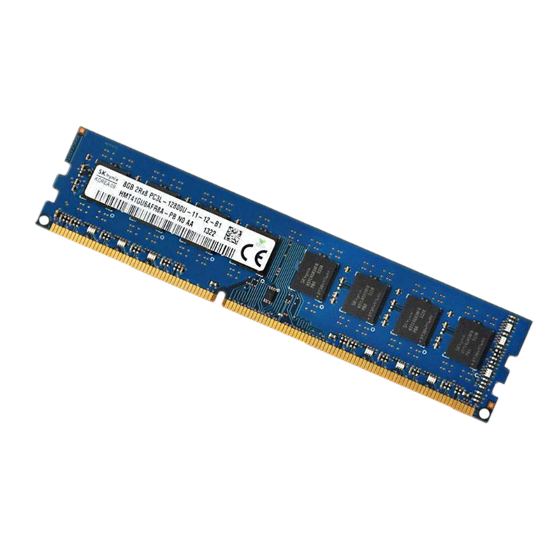
-Golden Finger PCB
Designed specifically for frequent plugging and unplugging scenarios such as memory modules and graphics cards, it requires high wear resistance, oxidation resistance, and conductivity, and is suitable for high-speed data transmission or high reliability connections.
-Ordinary PCB
mostly used for fixing soldering components (such as resistors and ICs), without considering insertion and removal wear, with lower cost.

2. Differences in materials and processes
-Coating material
Gold fingers are coated with hard gold (containing cobalt or nickel), while ordinary solder pads are often coated with immersion gold (low cost) or OSP (organic solder mask).
-Structural complexity
Gold fingers require additional process steps (such as chamfering, copper cutting, solder mask opening), while the pad design of ordinary PCBs is more simplified.
3. Electrical performance requirements
-Signal integrity
Gold fingers require strict impedance control (such as copper cutting), while impedance control for ordinary PCBs is mostly focused on inner layer wiring.
-Environmental resistance
Gold fingers need to adapt to multiple insertions and mechanical stresses, while ordinary PCBs focus more on long-term soldering reliability.
4. Cost and manufacturing cycle
-Due to the gold plating process and complex processing steps, the cost of gold finger is significantly higher than that of ordinary PCB, and it requires higher processing accuracy from the board factory (such as a bevel angle error of ≤ 0.1mm).
3、 Summary
So,How to design gold finger PCB?The design of Golden Finger PCB requires strict adherence to specifications in layout, plating, inner layer treatment, and testing. Its core differences from ordinary PCBs lie in application scenarios, material selection, and process complexity. Designers need to choose a suitable solution based on specific requirements such as insertion and extraction frequency, signal speed, and cost budget. For example, high-frequency devices require multi-layer boards and segmented gold fingers, while ordinary consumer electronics may prefer traditional solder pads to reduce costs.