Table of Contents
Introduction to CIS Technology
CMOS Image Sensors (CIS) have revolutionized digital imaging across countless applications, from smartphone cameras to automotive vision systems. These sophisticated semiconductor devices convert incoming light into electronic signals, enabling the capture of visual information in digital form . As CIS technology continues to advance with higher pixel counts, faster frame rates, and improved sensitivity, the printed circuit boards that support these sensors face increasingly complex design challenges. For PCB manufacturers, understanding the unique requirements of CIS applications is essential for delivering reliable, high-performance solutions that meet the demanding standards of today’s imaging applications.
This article explores the key considerations for PCB design and manufacturing in CIS-based systems, addressing technical challenges and presenting innovative solutions that balance performance, size, power efficiency, and reliability.
1.Technical Evolution and Market Applications of CIS
From Consumer Electronics to Critical Systems
CIS technology has expanded far beyond its initial applications in consumer photography. Today, these sensors serve diverse markets with varying reliability and performance requirements:
•Consumer Electronics: Smartphones employ multiple CIS units for front and rear cameras, with increasing pixel counts and decreasing form factors . Modern flagship phones typically incorporate two to six cameras, each requiring specialized PCB support .
•Automotive Systems: Advanced driver assistance systems (ADAS) and autonomous driving technologies utilize numerous exterior and interior cameras for comprehensive environmental monitoring . The upcoming Sony IMX828 sensor, for instance, represents the cutting edge with integrated MIPI A-PHY interface for automotive applications .
•Industrial and Medical Imaging: Machine vision, industrial inspection, and medical diagnostic equipment rely on CIS for precise image capture in specialized environments .
•Emerging Applications: Augmented/virtual reality (AR/VR), security systems, and IoT devices continue to drive innovation in CIS technology .

2.Key PCB Design Challenges for CIS Applications
Miniaturization and Component Density
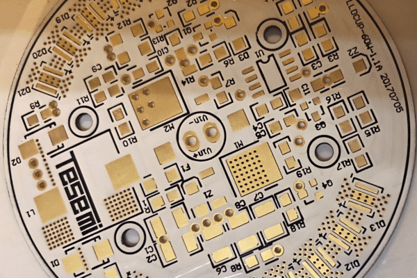
As consumer devices trend toward thinner form factors, PCB real estate has become increasingly constrained. Smartphone front camera PCBs, for example, must typically fit within dimensions as small as 10mm × 8mm while accommodating the sensor, ISP chip, LED drive circuitry, and supporting components . This extreme miniaturization demands advanced PCB technologies like high-density interconnect (HDI) with micro-vias and finer trace widths .
Signal Integrity at High Data Rates
Modern CIS components output massive data streams through high-speed interfaces like MIPI C-PHY, which can operate at rates up to 8Gbps . At these frequencies, traditional FR-4 substrates exhibit significant signal attenuation—approximately 1.2dB per centimeter at 8Gbps . This loss manifests as image noise, edge blurring, and color inaccuracies in the final output, necessitating specialized materials and careful impedance control.
Power Integrity and Thermal Management
Higher resolution sensors consume substantial power—up to 800mW for 48-megapixel modules in some smartphone applications . This power dissipation creates thermal challenges in compact designs where heat buildup can degrade image quality and potentially trigger thermal protection mechanisms that reduce resolution . Effective power delivery and thermal dissipation are therefore critical considerations in CIS PCB design.
Electromagnetic Compatibility
In complex electronic assemblies, CIS circuits are vulnerable to electromagnetic interference from nearby components like Wi-Fi and Bluetooth modules . Additionally, the high-speed signals from the image sensor can themselves become sources of electromagnetic emissions, potentially affecting other system components and complicating regulatory compliance .
3.Advanced PCB Solutions for CIS Applications
HDI Technology for Miniaturization
To address space constraints while maintaining functionality, high-density interconnect (HDI) technology offers several advantages:
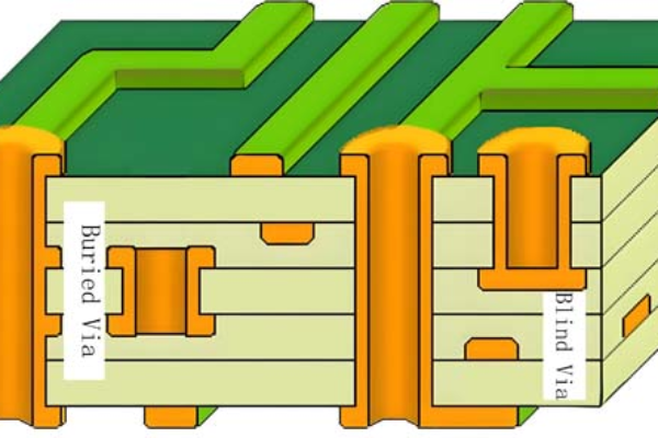
•Micro-via Architectures: Using blind vias with diameters as small as 0.1mm and buried vias of 0.15mm reduces via capture pad sizes and increases routing density . This enables component placement on both sides of the PCB, effectively implementing a “3D” component arrangement.
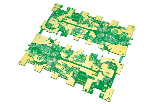
•High Layer Counts: While conventional designs might use 4 layers, advanced CIS PCBs employ 8-10 layer stackups with sequential lamination processes to achieve sufficient routing channels in minimal thickness .
•Fine-Pitch Components: HDI processes support miniature 01005-size passive components (0.4mm × 0.2mm) and wafer-level chip-scale package (WLCSP) ICs with pitches as tight as 0.3mm .
Table: HDI PCB Capabilities for CIS Applications
| Parameter | Standard PCB | Advanced HDI for CIS |
| Minimum Via Size | 0.2mm | 0.1mm |
| Line Width/Spacing | 0.1mm/0.1mm | 0.05mm/0.05mm |
| Component Size | 0201 (0.6mm × 0.3mm) | 01005 (0.4mm × 0.2mm) |
| Maximum Layer Count | 6-8 | 10-12+ |
| PCB Thickness | 1.2mm | 0.7-0.8mm |
High-Frequency Materials for Signal Integrity
To maintain signal integrity at multi-gigabit data rates, specialized PCB materials offer superior performance:
•Low-Loss Laminates: Materials like Rogers RO4350B (tanδ ≤ 0.004) or ShengYi S1000-2 (tanδ ≤ 0.008) significantly reduce high-frequency attenuation compared to standard FR-4 (tanδ ≈ 0.02) .
•Controlled Impedance: Careful stackup design and manufacturing process control maintain tight impedance tolerances—typically 50Ω ±3% for MIPI differential pairs .
•Transmission Line Optimization: Proper differential pair routing with matched lengths (length mismatches ≤ 0.2mm), appropriate termination, and minimal via transitions preserve signal quality .
Power Delivery and Thermal Management
Successful CIS implementations incorporate multiple strategies for power and thermal management:
•Efficient Power Conversion: Using low-quiescent-current power management ICs like the TI TPS62740 with efficiencies ≥ 90% minimizes conversion losses and reduces overall power consumption .
•Dynamic Power Control: Implementing multi-mode operation—with separate “standby,” “wake,” and “active” states—significantly reduces average power consumption . Some designs report power reductions from 65mW to 42mW in typical use cases .
•Thermal Via Arrays: Placing thermal vias with 0.3mm diameters at 1mm pitch beneath heat-generating components like ISP chips conducts heat to internal ground planes or opposite-side copper pours .
•Copper Heat Spreading: Incorporating defined copper areas (with typical 0.2mm trace width and 0.5mm spacing) on outer layers improves heat dissipation .
EMI Mitigation Techniques
Managing electromagnetic compatibility requires a multi-faceted approach:
•Segregation and Isolation: Physically separating “clean” analog/image signal areas from “noisy” digital circuits using ≥2mm wide grounded guard traces with 1oz copper thickness reduces cross-coupling .
•Component Selection: Strategic use of ferrite beads with impedance of at least 1kΩ at 100MHz or common-mode chokes on input lines suppresses high-frequency noise .
•Shielding: Employing 0.1mm aluminum shields over sensitive areas or noisy circuits, properly grounded to the PCB, contains EMI at its source .
4.Automotive CIS: Specialized Requirements and Solutions
The automotive environment presents unique challenges for CIS PCB design, with solutions exemplified by cutting-edge components like the Sony IMX828:
•Integrated Interfaces: Newer sensors like the IMX828 incorporate MIPI A-PHY interfaces directly, eliminating the need for external serializers and simplifying the surrounding PCB design . This integration reduces component count, saves board space, and lowers power consumption.
•Enhanced Reliability: Automotive CIS PCBs must withstand harsh operating conditions while maintaining signal integrity. This requires materials with stable electrical properties across temperature extremes and robust mechanical construction to resist vibration and shock.
•Functional Safety: PCBs for automotive vision systems must support implementation of functional safety features, with designs complying with ISO 26262 standards .

5.Future Trends and Development Directions
CIS technology continues to evolve, driving corresponding advances in PCB design and manufacturing:
•Higher Resolution Sensors: As pixel counts increase beyond current 48-megapixel consumer sensors and 8-megapixel automotive sensors, PCB designs must support even higher data rates while managing increased power density.
•Multi-Sensor Integration: Systems incorporating multiple CIS units for computational photography or 3D sensing will require PCBs that can accommodate several sensors with minimal interference.
•Advanced Packaging Technologies: Approaches like system-in-package (SiP) and embedded components will further reduce form factors while potentially moving some traditional PCB functions into the sensor package itself.
•Material Innovations: Ongoing development of PCB substrates with improved dielectric properties will enable better signal integrity at higher frequencies with reduced loss.
Conclusion: Partnering for CIS Success
Designing and manufacturing PCBs for CMOS Image Sensor applications requires specialized expertise in high-speed digital design, miniaturization techniques, thermal management, and signal integrity preservation. As CIS technology advances toward higher resolutions, faster frame rates, and broader application across industries, the supporting PCB infrastructure must evolve correspondingly.
Successful CIS implementations demand:
•Expertise in HDI technologies for space-constrained applications
•Understanding of high-frequency materials and controlled impedance techniques
•Knowledge of thermal management strategies for power-dense designs
•Experience with EMI mitigation for electromagnetic compatibility
•Familiarity with industry-specific standards for automotive, medical, or industrial applications
For PCB manufacturers, developing these specialized capabilities creates significant opportunities to add value in the growing imaging ecosystem. By partnering with customers to address the unique challenges of CIS-based systems, PCB companies can position themselves as essential enablers of next-generation imaging applications across consumer, automotive, industrial, and medical markets.
Embrace the evolving landscape of CIS technology with PCB solutions that balance performance, size, power efficiency, and cost-effectiveness—delivering the image quality and reliability that modern applications demand.