

Table of Contents
Executive Summary
Embedded PCB technology represents a revolutionary approach in circuit board design and manufacturing, where active and passive components are integrated directly within the inner layers of the printed circuit board structure. This advanced packaging methodology delivers significant advantages over traditional surface-mounted approaches, including enhanced performance, reduced form factors, and improved reliability. As electronic devices continue to evolve toward miniaturization and increased functionality, embedded PCB technology has emerged as a critical enabler across various industries, from consumer electronics and automotive systems to medical devices and industrial applications. This comprehensive guide explores the fundamental concepts, design considerations, manufacturing processes, and future trends of embedded PCB technology, providing valuable insights for electronics manufacturers and designers seeking to leverage this innovative approach.
1. Introduction to Embedded PCB Technology
1.1 Fundamental Concepts
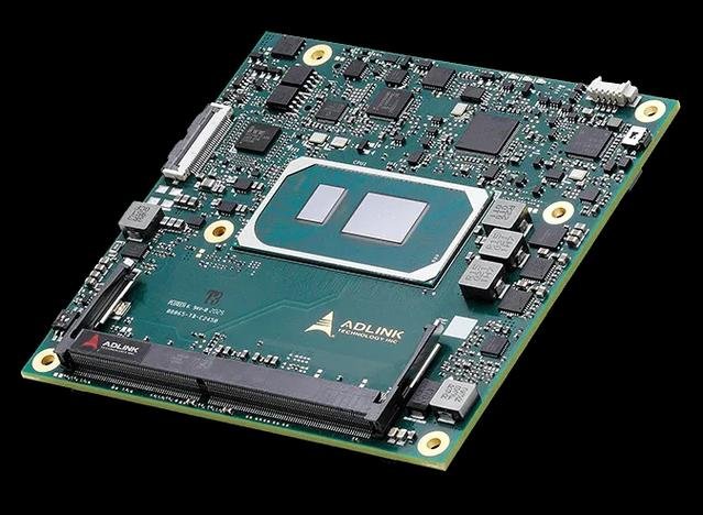
Embedded PCB technology fundamentally transforms traditional circuit board architecture by integrating electronic components within the multilayer structure of the board itself, rather than mounting them on the surface . This innovative approach represents a significant departure from conventional PCB manufacturing methods and offers new possibilities for electronic product design. The technology encompasses both embedded active components (such as integrated circuits and transistors) and embedded passive components (including resistors, capacitors, and inductors) within the PCB’s internal layers, creating a more compact and efficient electronic assembly.
The concept of embedding components within substrate assemblies is not entirely new, particularly for low-power and logic device packaging where it has reached a high level of maturity . However, recent advancements in materials, manufacturing processes, and design methodologies have expanded the applications and capabilities of embedded PCB technology, making it increasingly viable for a broader range of electronic products and industries.
1.2 Historical Development and Evolution
The evolution of embedded PCB technology parallels the broader trend toward electronic miniaturization and functional integration in the electronics industry. Early implementations focused primarily on embedding passive components to save surface space and improve electrical performance. As manufacturing capabilities advanced, the technology progressed to include more complex active components, driven by ongoing demands for smaller, faster, and more reliable electronic devices.
Significant milestones in this evolution include the development of MicroSIP™ packaging by Texas Instruments and AT&S, as well as BLADE™ packaging from Infineon, which demonstrated the feasibility of high-volume production using embedded PCB technology . These early successes paved the way for broader industry adoption and continued technological refinement, establishing embedded PCB as a viable packaging solution for various applications.
2. Key Advantages of Embedded PCB Technology
2.1 Enhanced Electrical Performance
Embedded PCB technology delivers substantial improvements in electrical performance compared to traditional surface-mounted approaches:
•Reduced Parasitic Effects: By minimizing interconnection lengths, embedded technology significantly decreases parasitic inductance and capacitance. This reduction is particularly beneficial for high-frequency applications, where parasitic elements can severely impact circuit performance .
•Improved Signal Integrity: The shorter electrical paths within embedded structures enhance signal integrity by reducing signal loss, reflection, and propagation delay. This advantage becomes increasingly critical as data rates continue to escalate in modern electronic systems.
•Lower Power Loop Inductance: Technologies like GaN Systems’ GaNpx™ packaging demonstrate how embedded approaches can achieve low inductance, small form factors, and reduced thermal resistance simultaneously. This integration enables cleaner switching waveforms with minimal voltage overshoot, even at high dV/dt rates .
2.2 Miniaturization and Space Efficiency
The three-dimensional integration capability of embedded PCB technology enables significant space savings:
•Increased Component Density: By utilizing the vertical dimension within the PCB structure, embedded technology allows for higher component density without increasing the board’s footprint. This advantage is particularly valuable for space-constrained applications such as mobile devices, wearables, and compact electronic systems.
•Reduced Form Factors: The elimination of surface-mounted components and their associated mounting structures enables thinner product designs while maintaining or even enhancing functionality.
•3D Packaging Capabilities: Embedded technology facilitates the stacking of components in three dimensions, optimizing space utilization beyond what is possible with conventional surface-mount technology .
2.3 Thermal Management Advantages
Embedded PCB technology offers improved thermal performance through several mechanisms:
•Enhanced Heat Dissipation: The integration of components within the PCB structure provides additional thermal pathways for heat dissipation. Some implementations incorporate thick copper layers (up to 400μm) that serve as effective heat spreaders, improving overall thermal management .
•Direct Thermal Connections: Embedded components can be directly connected to thermal vias or heat-spreading layers, creating efficient thermal paths that reduce junction temperatures and enhance reliability.
•Dual-Side Cooling Possibilities: Symmetrically constructed embedded assemblies can facilitate cooling from both sides of the board, potentially doubling the available cooling surface area and improving thermal performance in high-power applications .
2.4 Reliability and Mechanical Stability
The structural integration of components within embedded PCBs delivers significant reliability benefits:
•Enhanced Mechanical Robustness: Embedded components are protected within the PCB structure, making them less susceptible to mechanical damage from impact, vibration, or other environmental stresses.
•Reduced Interconnection Failures: The elimination of many solder joints associated with surface mounting decreases potential failure points, enhancing the overall reliability of the electronic assembly.
•Improved Resistance to Environmental Factors: Encapsulating components within the PCB structure provides inherent protection against moisture, contaminants, and other environmental factors that can compromise electronic reliability.
3. Embedded PCB Design Considerations
3.1 Material Selection and Properties
Choosing appropriate materials is critical for successful embedded PCB implementation:
•Dielectric Materials: The selection of dielectric materials must consider thermal stability, dielectric constant, loss tangent, and compatibility with embedding processes. While standard FR-4 materials are sometimes used, their relatively low thermal conductivity (approximately 0.3 W/mK) may necessitate additional thermal management strategies .
•Copper Foils: The thickness and type of copper foils impact both electrical and thermal performance. Designs may incorporate varying copper thicknesses (from 35μm for fine-pitch routing to 400μm for high-current paths and thermal management) to optimize overall performance .
•Thermal Interface Materials: For applications requiring enhanced thermal performance, specialized materials with higher thermal conductivity may be incorporated to facilitate heat transfer from embedded components.
3.2 Thermal Management Strategies
Effective thermal management is essential for reliable embedded PCB operation:
•Thermal Via Arrays: Strategically placed thermal vias help transfer heat from embedded components to external heat sinks or spreading layers. The design of these via arrays must balance thermal performance with structural integrity and routing constraints.
•Copper Thickness Optimization: Thick copper layers (e.g., 100μm base foils or 400μm specialized layers) can be incorporated to enhance lateral heat spreading and improve overall thermal performance .
•CTE Matching: Managing coefficients of thermal expansion (CTE) between different materials is crucial for reliability. Mis-matched CTEs can generate significant thermomechanical stress, potentially leading to failure. Approaches include using ceramic substrates like AlN for better CTE matching with silicon chips, or implementing symmetrical layer stackups to balance stresses .
3.3 Signal and Power Integrity
Maintaining signal and power integrity presents unique challenges in embedded PCB design:
•Controlled Impedance: As signal speeds increase, careful control of impedance through precise dimensional management becomes essential. This control requires consideration of dielectric thickness, copper geometry, and material properties.
•Power Delivery Network (PDN) Design: The PDN must provide stable voltage with low noise to embedded components. This often requires specialized stackup designs with dedicated power planes and strategic decoupling capacitor placement.
•EMI Mitigation: The compact nature of embedded structures can help reduce electromagnetic interference (EMI) by minimizing loop areas. Additional techniques such as shielding layers between specific circuits may be incorporated to further control EMI .
4. Manufacturing Processes for Embedded PCBs
4.1 Core Manufacturing Methodologies
Embedded PCB fabrication involves specialized processes that differ from conventional PCB manufacturing:
•Component Placement and Fixation: The process begins with precisely placing components onto inner layer substrates using specialized equipment capable of high-accuracy positioning. Components are temporarily fixed using adhesives or other bonding methods before the lamination process.
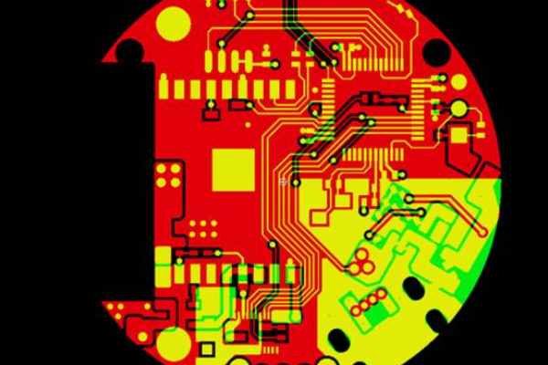
•Lamination and Layer Building: Multiple circuit layers with embedded components are stacked together with prepreg (pre-impregnated) dielectric materials and pressed under controlled temperature and pressure. This lamination process creates a solid, integrated structure with components encapsulated within.
•Via Formation and Interconnection: Various types of vias, including blind, buried, and through-hole vias, are created to establish electrical connections between layers. Laser drilling is commonly used for creating microvias with high precision and aspect ratios.
4.2 Specialized Techniques and Variations
Different approaches have been developed to address specific application requirements:
•Schweizer’s p²PACK™ Embedding Method: This approach utilizes pre-tested standard cells (S-Cells) that are placed into precisely formed cavities within the PCB lamination . The method has been successfully validated in volume production for 48V MOSFET technology, demonstrating a 35% performance improvement over conventional approaches.
•AT&S Embedded Component Packaging (ECP®): This technology has been applied to various products, including smartphones and medical devices, demonstrating its versatility across different applications .
•Mitsubishi’s 3D Integration Approach: This methodology enables the symmetrical arrangement of components like SiC MOSFETs within the PCB structure, with integrated gate drivers and specialized copper layer arrangements for optimized performance .
5. Applications and Use Cases
5.1 Automotive Electronics
The automotive industry represents a significant application area for embedded PCB technology:
•Power Conversion Systems: Embedded technology is particularly suited for automotive power electronics, including DC-DC converters and traction inverters. The demonstrated ability to achieve power loop inductances as low as 2.3 nH enables cleaner switching waveforms with reduced voltage overshoot, even at high dV/dt rates exceeding 90 V/ns .
•Advanced Driver Assistance Systems (ADAS): The miniaturization, improved thermal performance, and enhanced reliability offered by embedded PCB technology make it well-suited for ADAS applications, where space constraints and demanding operating conditions are common challenges.
•Electric Vehicle Powertrains: The efficiency benefits of embedded technology, combined with its ability to handle high power levels, position it as an enabling technology for electric vehicle powertrain components .
5.2 Consumer Electronics
Consumer products benefit significantly from the miniaturization and performance advantages of embedded PCBs:
•Mobile Devices: Smartphones, tablets, and wearables leverage embedded technology to achieve increasingly compact form factors while maintaining or enhancing functionality.
•Portable Electronics: The space efficiency and improved reliability of embedded PCBs make them ideal for various portable electronic devices where size, weight, and durability are key considerations.
5.3 Industrial and Medical Applications
Demanding industrial and medical environments increasingly adopt embedded PCB technology:
•Industrial Control Systems: The enhanced reliability and robust performance of embedded PCBs under challenging operating conditions make them suitable for industrial control applications.
•Medical Devices: Medical electronics benefit from the miniaturization, reliability, and performance advantages of embedded technology, particularly for portable medical equipment and implantable devices.
•Power Electronics: Applications such as motor drives, power supplies, and energy conversion systems benefit from the improved electrical and thermal performance offered by embedded PCB approaches.
6. Comparative Analysis: Embedded vs. Traditional PCB Technologies
6.1 Performance Comparison
Embedded PCB technology offers several performance advantages over traditional approaches:
•Size and Weight: Embedded technology typically enables 30-50% reduction in board space utilization compared to conventional surface-mount technology, with corresponding weight reductions.
•Electrical Performance: Significantly lower parasitic elements (inductance and capacitance) improve high-frequency performance, with demonstrated power loop inductance reductions to 2-3 nH compared to 10+ nH for conventional approaches .
•Thermal Management: The integrated structure of embedded PCBs provides better thermal paths, with thermal resistance improvements of up to 50% compared to discrete packages in some implementations.
6.2 Economic Considerations
The economic implications of embedded PCB technology include both costs and benefits:
•Manufacturing Costs: Embedded PCBs typically involve higher manufacturing costs due to process complexity and specialized equipment requirements. However, these costs may be offset by system-level savings, including reduced board size, simplified assembly, and improved yield.
•Value Proposition: The business case for embedded technology strengthens in applications where performance, size, or reliability requirements justify the additional manufacturing expense. This is particularly true in automotive, medical, and high-reliability industrial applications.
7. Future Trends and Developments
7.1 Technological Advancements
Several emerging trends are shaping the future evolution of embedded PCB technology:
•Advanced Materials: Development of new dielectric materials with improved thermal and electrical properties will enable higher-performance embedded solutions. Materials with higher thermal conductivity and tailored dielectric constants will address current limitations.
•Heterogeneous Integration: The integration of diverse technologies, including silicon, wide-bandgap semiconductors, and passive components, within a single embedded structure will create more sophisticated and capable systems.
•Additive Manufacturing: Advancements in additive processes for electronics fabrication may complement or enhance traditional embedded PCB manufacturing methods, potentially enabling new design possibilities.
7.2 Market Growth and Adoption
The embedded PCB market shows significant growth potential across multiple sectors:
•Market Expansion: According to market research, the embedded PCB sector is expected to experience substantial growth, driven by increasing adoption across automotive, consumer, and industrial applications .
•Application Diversification: While currently concentrated in specific high-value applications, embedded PCB technology is expected to expand into broader market segments as manufacturing processes mature and costs decrease.
8. Conclusion
Embedded PCB technology represents a significant advancement in electronic circuit design and manufacturing, offering compelling advantages in performance, miniaturization, and reliability. While presenting design and manufacturing challenges, the technology enables innovative solutions across diverse applications, from automotive systems to consumer electronics and medical devices.
As electronic products continue to evolve toward increased functionality in smaller form factors, embedded PCB technology is poised to play an increasingly important role in enabling these advancements. For PCB manufacturers and electronic product developers, understanding and leveraging this technology will be essential for maintaining competitiveness in an increasingly demanding marketplace.
The ongoing development of materials, processes, and design methodologies will likely address current limitations while expanding the application space for embedded PCB technology. By embracing this innovative approach, electronics manufacturers can create more advanced, reliable, and compact electronic products that meet the evolving needs of the market.
Partner with Us for Your Embedded PCB Projects
Our expertise in advanced PCB manufacturing and embedded technology ensures that your designs leverage the full potential of this innovative approach. With specialized capabilities in complex multilayer designs, precision component embedding, and rigorous testing protocols, we deliver solutions that excel in performance and reliability.
Contact us today to discuss how we can support your embedded PCB projects with cutting-edge technology tailored for your specific application requirements.
-600x400-c.png)