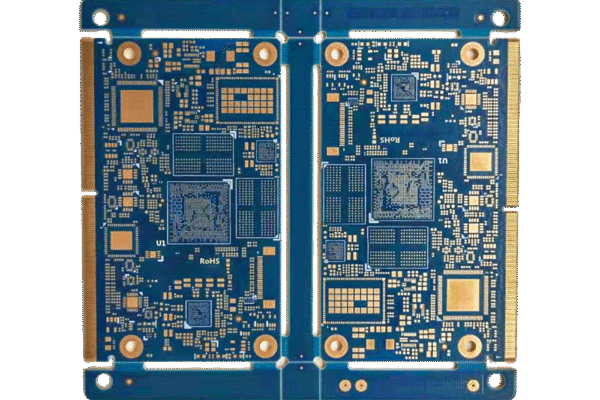
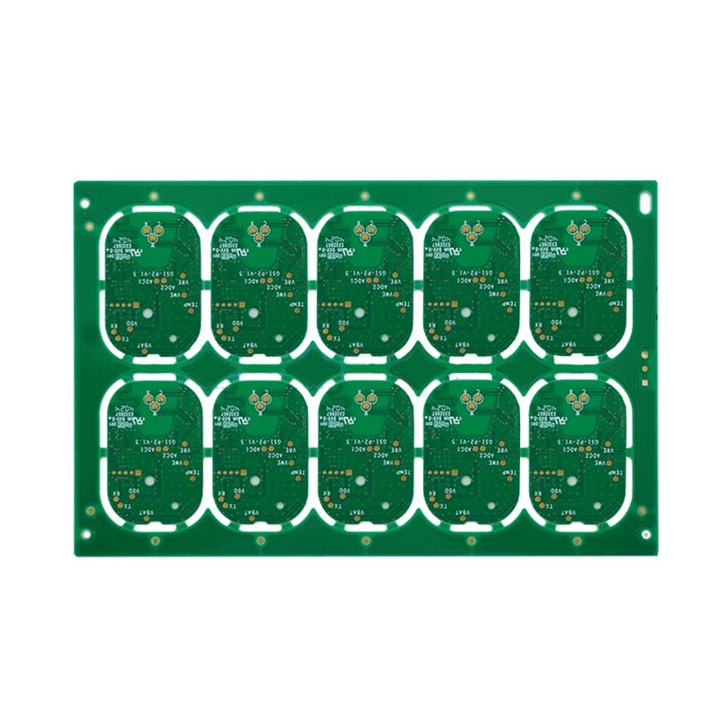
OSP (Organic Solderability Preservative) is a surface treatment process that forms an organic film on the surface of a printed circuit board (PCB), mainly used to protect copper foil from oxidation while ensuring good solderability. The following is a detailed analysis of its advantages and disadvantages:
Table of Contents
Ⅰ. Advantages of OSP
1. Low cost
-The process is simple, does not require expensive equipment (such as electroplating lines), has low material costs and energy consumption, and is suitable for large-scale production, especially with significant advantages for low-cost PCBs (such as consumer electronics and home appliances).
2. High flatness of solder pads
-The formed protective film has an extremely thin thickness (usually 0.2-0.5 μ m), which hardly changes the surface flatness of the solder pad, making it conducive to precision welding (such as fine pitch components and BGA packaging) and avoiding welding defects caused by uneven coating thickness.
3. Excellent weldability
-The protective film will quickly decompose during welding, exposing the fresh copper surface and directly reacting with solder (such as solder paste) to form reliable solder joints, resulting in high welding yield.
4. Strong compatibility
-Friendly to subsequent processes such as mounting and repair, compatible with various soldering methods such as wave soldering and reflow soldering, and less prone to adverse reactions with flux.
5. Good environmental friendliness
-Does not contain harmful substances such as lead and nickel, complies with environmental standards such as RoHS, has simple wastewater treatment, and low environmental pollution risk.
6. Suitable for high-frequency/high-speed signals
-The film layer does not affect the electrical performance of the PCB (such as impedance matching), making it particularly suitable for high-frequency circuits and high-speed signal transmission scenarios (such as communication equipment and server motherboards).
Ⅱ. Disadvantages of OSP
1. Short storage cycle

-The protective film is prone to moisture absorption and long-term exposure to air may cause slight oxidation, leading to a decrease in weldability. The usual storage period is 3-6 months (in a dry environment), and if exceeded, it needs to be reprocessed.
2. Poor mechanical resistance
-The film layer is thin and fragile, unable to resist physical damage during friction, scratching, or handling, and may result in exposed oxidation of the copper surface due to improper operation.
3. Not compatible with manual welding/multiple welding
-The single welding effect is ideal, but when welding multiple times (such as repair), the protective film may completely decompose, and the oxidation rate of the copper surface may accelerate, requiring additional use of flux or reprocessing of the solder pads.
4. Unable to cover non pad areas
-It can only protect the solder pads and copper foil, and has no protective effect on non solder pad areas such as through holes and copper plated holes, which may affect the reliability of interlayer connections in multilayer boards.
5. Incompatible with some surface treatments
-If secondary processing is required (such as gold plating or nickel plating), the OSP film needs to be removed first, which increases the complexity of the process; In addition, it is not suitable for direct contact with materials such as silver paste and conductive adhesive, which may cause chemical reactions.
6. Difficulty in appearance inspection
-The film layer is colorless and transparent, making it difficult to determine whether it is uniformly covered or has defects through visual inspection. It requires the use of AOI (Automatic Optical Inspection) or contact resistance testing.
Ⅲ.Application scenarios and alternative solutions
-Applicable scenarios:
-Low cost, short cycle consumer electronics products (such as mobile phone motherboards, laptop PCBs).
-High frequency circuits and thin PCBs with high precision welding requirements.
-Export products with strict environmental requirements.
-Alternative solution:
-ENIG: High reliability, long storage cycle, suitable for high reliability products (such as automotive electronics, industrial control), but with high cost.
-HASL: Low cost, good solderability, but poor flatness, not suitable for precision components.
-Chemical nickel gold plating (ENEPIG): It has both flatness and wear resistance, and is used for high-end communication equipment, but the process is complex.

Summarize
OSP has become one of the mainstream surface treatment processes due to its low cost, high flatness, and environmental friendliness, but its limitations in storage resistance and mechanical properties make it more suitable for short-term production and specific scenarios. When selecting, a comprehensive evaluation should be conducted based on product reliability requirements, process complexity, and cost budget.