As an indispensable carrier of electronic products, printed circuit boards (PCBs) are known as the “mother of the electronics industry”. This article will deeply analyze the core definition, technical characteristics, and strategic position of PCB in technological development, helping you fully understand the value code of this fundamental component.
Table of Contents
1、 Definition and Evolution of PCB
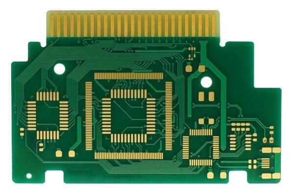
PCB is an electronic component carrier that forms conductive paths on an insulating substrate through etching process. Its core functions include:
1. Electrical Interconnection: Copper foil circuits enable signal transmission and power supply between components;

2. Mechanical support: Epoxy resin and other substrates provide physical fixation for components;
3. System integration: Multi layer stacking design meets high-density circuit requirements.
Since its birth in the early 20th century, PCB has undergone technological leaps from single-layer boards to HDI high-density interconnects, becoming the underlying supporting technology for cutting-edge fields such as 5G communication and artificial intelligence. It is predicted that the global PCB market size will exceed 100 billion US dollars by 2026, with China accounting for over 50%, highlighting its core position in the industry.
2、 The Five Core Characteristics of PCB
1. Material diversity
-Basic substrate: FR-4 epoxy glass fiber board dominates due to its high cost-effectiveness;
-Special scenario: Flexible Printed Circuit (FPC) adapts to the folding needs of wearable devices, while metal substrates enhance heat dissipation efficiency;
-High frequency application: Rogers board ensures the stability of 5G millimeter wave signal transmission.
2. Design optimizability
-Signal integrity: Adjust timing through wiring strategies such as serpentine lines, and suppress electromagnetic interference through differential routing;
-Thermal management: Copper block embedding and thick copper design optimize the heat dissipation path to avoid high-temperature failure.
3. Process precision
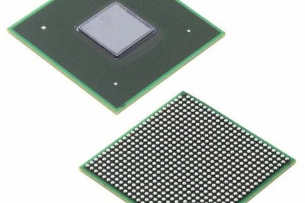
-Laser positioning system is used for multi-layer boards with more than 8 layers, and the interlayer alignment accuracy reaches ± 25 μ m;

-The precision of HDI board micro hole processing has exceeded 0.1mm, and the roughness of the hole wall has been controlled to Ra<0.8 μ m.
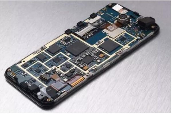
4. Application universality
Covering nine major fields including consumer electronics (mobile phone/computer motherboards), automotive electronics (ADAS control systems), medical equipment (CT scanners), etc., supporting 70% of global electronic device operations.
5. Environmental sustainability
Lead free soldering technology reduces heavy metal pollution, biodegradable substrate research and development promotes green manufacturing, and the metal recycling rate of waste PCB reaches over 90%.
3、 The strategic importance of PCB
1. The driving force behind technological upgrades
-High density interconnect (HDI) technology helps to miniaturize chip packaging;
-Intelligent PCB integrated sensors empower IoT devices to make autonomous decisions.
2. The cornerstone of industrial economy
-China’s PCB output value accounts for 54% of the world’s total, driving the upstream and downstream industry chain worth billions of yuan;

-The demand for automotive electronic PCBs is increasing by 12% annually, driving innovation in new energy vehicles.
3. The lifeline of reliability
-The IPC Class 3 standard ensures the stability of aerospace PCBs in extreme environments;
-22 quality inspection processes ensure 100000 hours of trouble free operation of industrial control boards.
Conclusion: Resonance with Future Technology on the Same Frequency
From smartphones to satellite communications, PCBs continue to push the limits of physics and drive innovation in the electronics industry. As a professional PCB manufacturer, we provide high-frequency high-speed board customization and full process DFM analysis to help you seize the technological high ground.