PCB (printed circuit board) wiring open circuit refers to the breakage or interruption of wires in the circuit, resulting in the inability of current to flow normally, thereby causing the circuit to malfunction. The following are common causes of open circuit in PCB wiring and corresponding improvement measures:
Table of Contents
Ⅰ. Reasons for PCB wiring open circuit
1. Issues during the design phase
-The wiring width is too narrow or the thickness is insufficient
-Too small a wire width can lead to insufficient current carrying capacity, and it may burn out due to heating after prolonged power on; Insufficient thickness (such as copper foil thickness being too thin) is also prone to fracture due to current stress.

-Unreasonable routing corner design
-Right or sharp corners are prone to stress concentration and may break during manufacturing or use; Uneven etching of copper foil at corners may also lead to open circuits.
-The wire spacing is too small or the connection with the solder pad is improper
-Insufficient spacing may result in thinning of the wiring due to excessive etching; If the transition between the solder pad and the wire connection is not smooth, it is easy to break under welding or stress.
-Defects in blind buried hole design
-The copper thickness of the blind buried hole wall is insufficient or the connection is poor, which may result in an open circuit at the interlayer conduction point.
2. Manufacturing process defects
-Excessive etching
-Excessive concentration of etching solution or prolonged etching time can result in a wire width smaller than the design value, or even complete etching.
-Drilling or milling edge damage
-During drilling, the deviation of the drill bit may break the inner layer routing; Excessive mechanical stress during the edge milling process leads to the breakage of the edge routing.
-Poor copper deposition process
-When copper is deposited through holes, the coating is uneven or there are bubbles, causing the copper layer on the hole wall to break, resulting in an open circuit between the layers.
-The problem of solder mask coverage
-Solder mask ink covers the solder pads or traces, causing poor soldering or local insulation of the traces, resulting in an open circuit.
3. The impact of welding and assembly processes
-Welding temperature too high or time too long
-High temperature soldering (such as wave soldering and reflow soldering) may cause oxidation, deformation, and even melting of the copper foil during wire routing.
-Excessive welding stress
-Pulling and pulling components or PCBs forcefully during manual soldering can cause breakage at the connection between the wiring and the solder pads.
-Improper installation of components
-Large components (such as transformers and connectors) generate stress due to thermal expansion and contraction after welding, causing open circuits by pulling and pulling the wiring.
4. Use environment and external factors
-Mechanical stress effect
-During installation, transportation, or use, PCBs are subjected to bending and compression, resulting in wire breakage, especially for thin copper foils or fine wires.
-Temperature changes and thermal cycling
-Frequent temperature fluctuations result in inconsistent thermal expansion coefficients between PCB substrate and copper foil, leading to fatigue fracture of wiring (especially in multi-layer boards).
-Corrosion or oxidation
-Moisture, acidic or alkaline gases, or pollutants in the environment can cause oxidation and corrosion of copper foil, leading to a gradual thinning of the wiring until it disconnects.
-Static or overcurrent impact
-Electrostatic discharge (ESD) or transient overcurrent may burn thin wires and form an open circuit.
Ⅱ.Improvement measures
1. Optimize the design plan

-Reasonable design of wiring width and thickness
-Calculate the wire width based on the current (for example, for 1A current, it is recommended to have a wire width of ≥ 1mm and a copper foil thickness of ≥ 1oz) to avoid being too thin; High power circuits can increase the thickness of copper foil or use multi-layer wiring in parallel.
-Improve corner and connection design
-The routing corner adopts a 45 ° or circular arc angle (as shown in the figure) to reduce stress concentration; The connection between the solder pad and the wiring adopts a Teardrop design to enhance the connection strength.
-Control the spacing between wiring and the layout between layers
-Wire spacing ≥ 0.1mm (adjusted according to PCB accuracy) to avoid mutual influence during etching; The inner layer routing should avoid overlapping with drilling and through holes.
-Optimize the design of through holes and blind buried holes
-Match the through-hole diameter with the pad size (e.g. 0.3mm aperture corresponds to 0.6mm pad), increase the copper thickness of the hole wall (≥ 25 μ m), and conduct reliability testing (such as thermal shock testing).
2. Improve the level of manufacturing technology
-Strictly control the etching process
-Monitor the concentration, temperature, and time of the etching solution, and use an automatic production line to reduce human error; Check the wire width after etching to ensure compliance with design requirements.
-Optimize drilling and milling processes
-Use a high-precision drilling rig, adjust the drill bit speed and feed rate to avoid hole displacement caused by drill bit wear; Numerical control equipment is used during edge milling to reduce PCB edge stress.
-Improving copper deposition and electroplating processes
-Thoroughly clean the hole wall before copper sinking through the through-hole to ensure that the coating is uniform and free of bubbles; Control the current density during electroplating to ensure that the thickness of the copper layer meets the standard.
-Standardize the production of solder mask layer
-When printing with solder mask ink, avoid covering the solder pads and critical traces, and follow the standard curing temperature and time to prevent ink residue from affecting the welding.
3. Standardize welding and assembly processes

-Control welding temperature and time
-The reflow soldering temperature curve is set according to the PCB material (such as FR-4, aluminum substrate) and component temperature resistance (such as peak temperature ≤ 230 ℃, duration ≤ 60s); Manual welding uses a constant temperature soldering iron (temperature ≤ 350 ℃, time ≤ 3s).
-Reduce welding stress
-Fix the PCB during welding to avoid shaking; Large components are fixed using brackets or adhesives to prevent thermal stress from pulling the wiring.
-Optimize component layout and installation
-Reserve sufficient heat dissipation space around high-power components (such as power resistors and ICs) to avoid wiring close to heat sources; The wiring of connectors and other load-bearing components should be as short and thick as possible to enhance their tensile resistance.
4. Strengthen the use environment and protective measures
-Reduce the impact of mechanical stress
-Use support columns or card slots during PCB installation to avoid hanging and bending; During transportation, use anti-static foam to wrap to prevent extrusion.
-Dealing with temperature and corrosive environments
-Choose heat-resistant substrates (such as polyimide) in high temperature environments, and coat the surface of the wiring with high-temperature resistant coatings; In humid or corrosive environments, PCB surfaces should be coated with three anti paints (moisture-proof, salt spray resistant, and mold resistant).
-Anti static and overcurrent protection
-Wear anti-static wristbands and floor mats during production and use; Add protective components such as TVS diodes and fuses in the circuit to prevent static electricity or overcurrent from burning out the wiring.
5. Strengthen quality inspection and reliability verification
-Manufacturing stage inspection
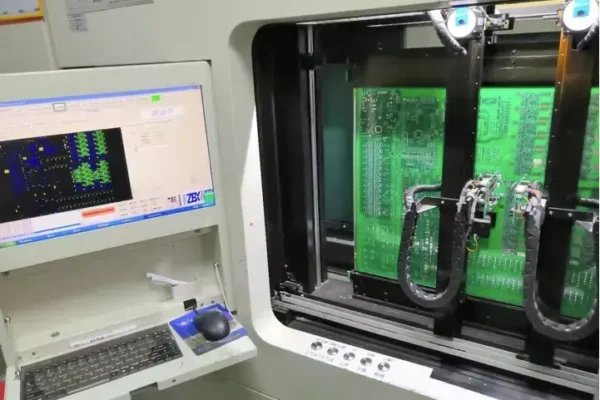
-Use flying needle testing or automatic optical inspection (AOI) to check the continuity of the wiring, and X-ray inspection to check the quality of blind buried hole welding.
-Reliability testing
-Perform thermal cycling test (-40 ℃~125 ℃, ≥ 100 times), bending test (deformation ≤ 0.5%), and voltage withstand test on PCB to detect potential open circuit risks in advance.
Ⅲ. Summary
The reasons for open circuit in PCB wiring cover multiple aspects such as design, manufacturing, assembly, and use. Improvement should start from the entire process: optimizing electrical and structural parameters at the design end, controlling process accuracy at the manufacturing end, standardizing operating procedures at the assembly end, and strengthening environmental protection at the usage end. By combining multidimensional measures, the risk of open circuit can be effectively reduced, and the reliability and service life of PCB can be improved.
Get your exclusive quote immediately: fill out the form or send an email directly.As a professional PCB manufacturer for hobbyist , we will provide you with a quote service within 24 hours. Enjoy free DFM optimization and a 10% discount on SMT patches for your first order!