Table of Contents
Introduction
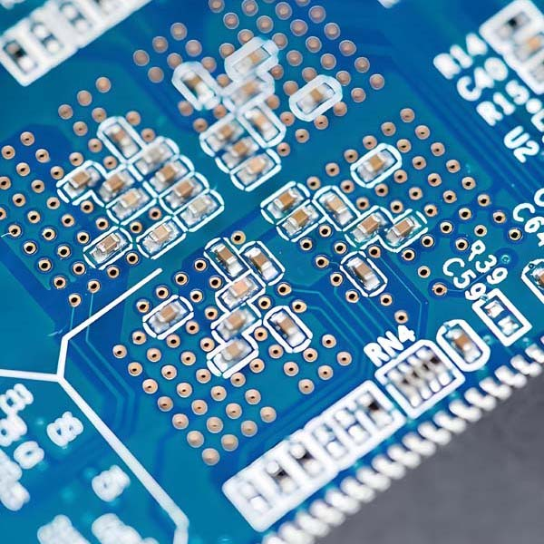
Ionic contamination on printed circuit boards (PCBs) refers to the presence of undesirable conductive residues—typically in the form of ions—that can compromise circuit performance and long-term reliability. These contaminants, often originating from manufacturing processes, human handling, or environmental factors, can lead to electrochemical migration (ECM), corrosion, and insulation failure. As electronics become more miniaturized and complex—with finer traces and higher component densities—the impact of even negligible contamination levels intensifies. This article explores the sources, mechanisms, and consequences of ionic contamination and outlines advanced detection and cleaning methodologies to ensure product integrity.
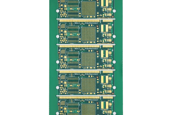
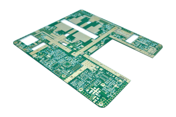
1. What is PCB Ionic Contamination?
Ionic contamination consists of charged residues (anions and cations) left on PCB surfaces or within layers after fabrication or assembly. These ions are electrically conductive under certain conditions and can initiate electrochemical reactions that degrade performance. Common ionic contaminants include:
– Anions: Chloride (Cl⁻), Bromide (Br⁻), Sulfate (SO₄²⁻), Nitrate (NO₃⁻), Weak Organic Acids (WOA)
– Cations: Sodium (Na⁺), Ammonium (NH₄⁺), Calcium (Ca²⁺), Potassium (K⁺)
These residues are typically measured in micrograms per square centimeter (μg/cm²) or micrograms per square inch (μg/in²), with stringent limits imposed by industry standards for high-reliability applications.
2. Primary Sources of Ionic Contamination
Ionic contaminants originate from multiple stages of PCB manufacturing and handling:
A. Fabrication Processes
•Etching & Cleaning Agents: Acidic or alkaline etchants (e.g., ammonium hydroxide, hydrochloric acid) leave behind ions like NH₄⁺, Cl⁻, SO₄²⁻.
•Surface Finishes: Processes like HASL (Hot Air Solder Leveling), ENIG (Electroless Nickel Immersion Gold), and OSP (Organic Solderability Preservative) can introduce halides or metal ions.
•Plate-Through Holes: Residual electrolytes from copper plating baths.
B. Assembly Operations
•Flux Residues: Wave soldering or reflow processes often involve fluxes containing brominated compounds, organic acids, or chlorinated activators.
•Solder Pastes: Some formulations may contain ionic surfactants or halide-based activators.
C. Human & Environmental Factors
•Fingerprints: Natural skin oils contain Na⁺, Cl⁻, and fatty acids.
•Pollution/Airborne Particles: Industrial environments can deposit sulfates or nitrates.
3. Consequences of Ionic Contamination
Left unchecked, ionic contamination can trigger catastrophic failures:
A. Electrochemical Migration (ECM)
Ions migrate between biased conductors in the presence of moisture, forming dendritic metallic growths (e.g., copper or silver) that cause short circuits and current leakage.
B. Corrosion
Reactive ions (e.g., Cl⁻) attack copper traces, solder joints, and component leads, leading to open circuits or intermittent connections.
C. Degraded Insulation Resistance
Conductive residues create leakage paths across insulating surfaces, reducing impedance and disrupting signal integrity.
D. Reduced Reliability & Lifespan
Devices operating in humid or high-temperature environments experience accelerated failure due to ion-driven degradation.
4. Detection and Measurement Standards
Accurate quantification of ionic contamination is essential for quality control. Key methods include:
A. Solvent Extraction (ROSE) Test
•Principle: Measures bulk resistivity of solvent extract (typically 75% IPA/25% DI water).
•Standard: IPC TM-650 2.3.25.
•Limitation: Does not identify specific ions.
B. Ion Chromatography (IC)
•Principle: Separates and quantifies individual anions/cations.
•Standard: IPC TM-650 2.3.28B.
•Advantage: High sensitivity and ion-specific data.
C. Industry Specifications
•General Electronics: ≤1.56 μg/cm² NaCl equivalence
•High-Reliability (Aerospace, Medical): ≤0.625 μg/cm²
5. Advanced Cleaning Technologies and Solutions
Effective removal of ionic contaminants requires tailored cleaning approaches:
A. Water-Based Cleaning Agents
•Mechanism: Utilize surfactants and chelators to dissolve and wash away ions.
•Examples:
–CZ-PCB-100A: High-concentration, low-foaming cleaner for喷锡, ENIG, OSP surfaces.
–ZP-380: Removes acidic ions, fluxes, and fingerprints; compatible with lead-free assemblies.
–W3210: pH-neutral cleaner for sensitive components and diverse soldering residues.
•Process: Spray or immersion at 50–65°C followed by DI water rinse and drying.
B. Dry Ice Blasting
•Mechanism: Uses solid CO₂ pellets to mechanically dislodge contaminants without chemicals.
•Benefits: Non-abrasive, residue-free, and effective for flux removal.
•Applications: PCBA post-solder cleaning.
C. Best Practices for Cleaning Process
•Pre-Cleaning Diagnosis: Use IC testing to identify specific ions for targeted cleaning.
•Material Compatibility: Ensure cleaners are safe for components, labels, and substrates.
•Environmental Control: Maintain cleanroom conditions to prevent recontamination.
•Waste Management: Treat effluent water to remove dissolved ions before disposal.
6. Prevention Strategies
Proactive measures minimize contamination introduction:
•Supplier Qualification: Audit PCB fabricators for ionic control practices.
•Process Optimization: Reduce flux usage and control soldering parameters.
•Handling Protocols: Enforce glove use and anti-static garments to prevent fingerprint contamination.
•Design for Cleanability: Avoid crevices and blind vias that trap residues.
7. Applications Demanding Stringent Control
•Aerospace & Defense: Harsh environments exacerbate ion-related failures.
•Automotive Electronics: Under-hood modules require long-term reliability.
•Medical Devices: Patient safety mandates ultra-low contamination levels.
•5G Infrastructure: High-frequency signals are sensitive to leakage currents.
Conclusion
PCB ionic contamination is an invisible threat with visible consequences. As electronic assemblies grow denser and applications more critical, robust contamination control becomes non-negotiable. Through a combination of rigorous process control, advanced cleaning technologies (e.g., water-based chemistry dry ice blasting), and precision metrology, manufacturers can ensure products meet the stringent reliability standards of modern electronics.
At SysPCB, we specialize in ionic contamination prevention and remediation. Our expertise in PCB materials, fabrication, and assembly processes helps clients achieve near-zero contamination levels for even the most demanding applications. Contact us to learn how we can enhance your product reliability.