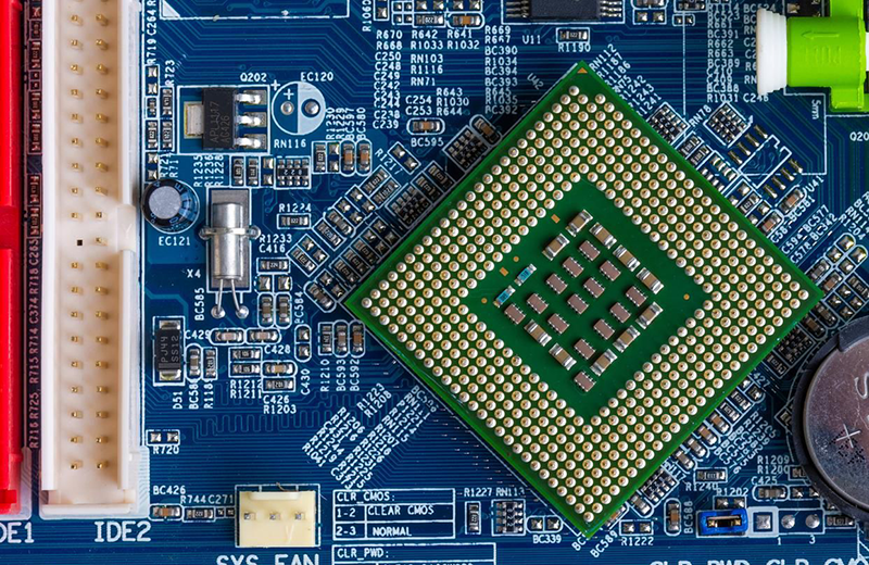
Hardware development is the cornerstone of electronic products, and its quality directly affects the performance and reliability of terminal devices. As the core link of integrated circuit design, SMT mounting, and PCB manufacturing, the global hardware development market has exceeded 300 billion US dollars, with China accounting for over 35%. This article will deeply analyze the four core elements of the entire hardware development process, showcasing technical details and industry value.
Table of Contents
1、 Hardware Design: From Requirement Definition to Precise Layout
1. Requirement analysis and indicator breakdown
Hardware design begins with precise requirement definition and requires comprehensive consideration of core indicators such as power consumption, size, and EMC (electromagnetic compatibility). For example, IoT devices require standby power consumption of less than 1mW, while industrial controllers need to meet IP67 protection level.
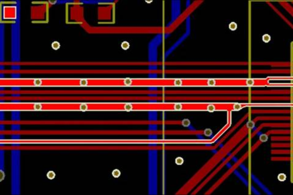
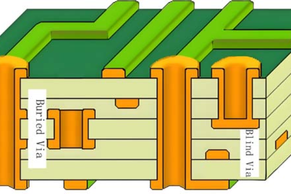
2. High density PCB design technology
-HDI process: adopting blind buried hole design to achieve 0.1mm micro hole interconnection on 8-layer board, increasing wiring density by 50%;
-Signal integrity optimization: Simulate DDR4 signals with HyperLynx tool to reduce crosstalk to within 5%;
-Thermal design management: By arranging a 2-ounce thick copper layer and a heat dissipation hole array, the chip junction temperature is controlled below 85 ° C.
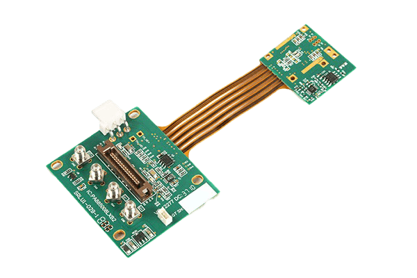
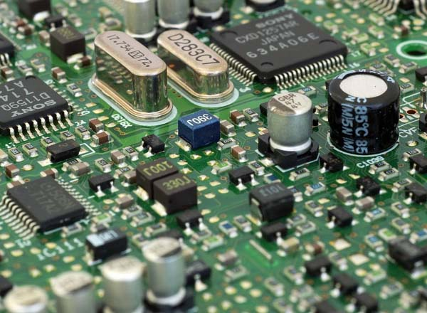
2、 Prototype manufacturing: precise implementation of SMT and PCB processes
1. Rapid prototyping ability
Support 24-hour delivery of 6-layer high-precision PCBs (gold plating process+impedance control) to help customers shorten their research and development cycle.
2. Breakthrough in SMT core process

-Micro component mounting: The component mounting accuracy of 01005 reaches ± 25 μ m, meeting the miniaturization needs of smart watches and other devices;
-Optimization of mixed packaging process: The stepped steel mesh technology solves the problem of BGA (0.4mm spacing) and QFN component co board printing;
-Advanced welding technology: Nitrogen reflow soldering reduces the oxidation defect rate of solder joints to below 0.02%.
3、 Test validation: Building a reliable moat
1. Strict environmental testing
-High and low temperature cycling (-40 ° C~125 ° C), vibration testing (20G acceleration, frequency 5-500Hz), simulating ten-year aging conditions;
-Damp heat test (85 ° C/85% RH, 1000 hours) to verify the moisture resistance of PCB.
2. Function and Certification System
-ATE automated testing: covering over 95% of circuit functions, with a false test rate of less than 0.1%;
-Industry specific certification: Passed standards such as ISO 26262 (Automotive Functional Safety) and IEC 60601-1 (Medical Electrical Safety).
4、 Mass production and industry empowerment: from standardization to customization
1. Mass production ramp up strategy
Through DFM (Design for Manufacturing) optimization, the SMT pass rate has been increased to over 98%, reducing customer production costs.
2. Vertical industry solutions
-Consumer electronics: 0.3mm ultra-thin flexible PCB+laser cutting technology, suitable for foldable screen mobile phone hinge area;
-Automotive electronics: 3-ounce thick copper PCB+three proof paint spray coating, meeting AEC-Q100 vibration and salt spray testing requirements;
-Industrial equipment: Aluminum substrate (thermal conductivity 2.0 W/m · K) solves the heat dissipation problem of 10kW frequency converter.
5、 Future trend: Technological innovation drives industry upgrading
1. Micro integration: SiP (System in Package) technology integrates SMT and wafer level packaging to achieve a 60% reduction in the volume of 5G modules;
2. Intelligent production line: AI real-time analysis of solder joint images (1000 frames per second), SPC control chart dynamically optimizes reflow soldering temperature zone parameters;
3. Green manufacturing: Halogen free substrate (Cl/Br<900ppm) and low VOC cleaning agent, in compliance with the EU REACH regulation.
Conclusion
Empowering hardware innovation with deep craftsmanship
Hardware development is a systematic engineering process that requires the accumulation of technology and experience at every stage, from design simulation to mass production delivery. As an SMT/PCB end-to-end service provider, we provide a one-stop solution from “design review – fast prototyping – certification support”, and have helped over 200 customers achieve successful mass production of their products.
Contact our hardware development team immediately to obtain customized technical solutions and industry case collections!