Gallium Nitride (GaN) has emerged as the cornerstone of next-generation power electronics, enabling unprecedented miniaturization and efficiency across consumer devices. As a wide bandgap semiconductor, GaN outperforms traditional silicon with superior switching speeds, higher thermal conductivity, and reduced energy losses—fundamentally reshaping power design paradigms. For consumer electronics brands, this translates to sleeker devices, faster charging, and eco-friendly energy savings.
Table of Contents
Why GaN Dominates Consumer Power Electronics
1.Extreme Miniaturization
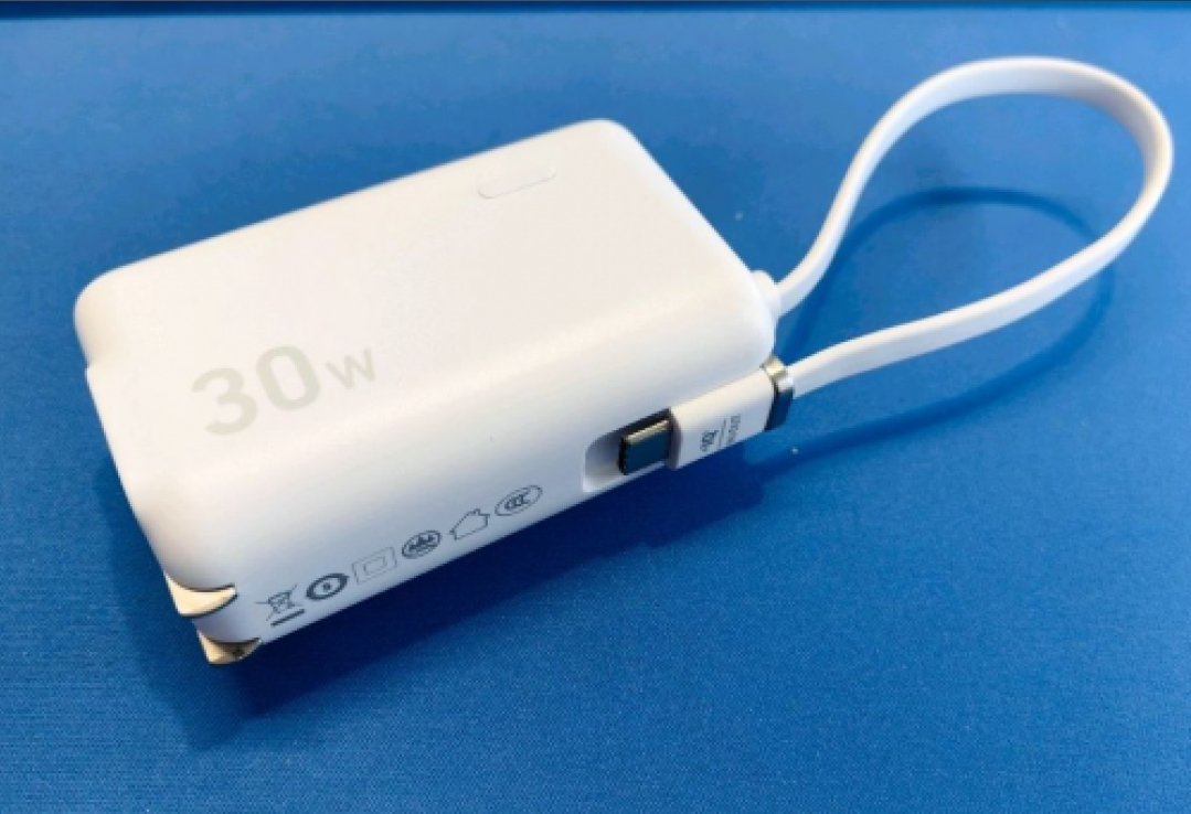
Gallium Nitride’s high electron mobility allows components to switch 100× faster than silicon, enabling smaller inductors/capacitors. Consumer chargers now achieve 40% size reduction at identical power levels (e.g., 65W chargers fitting in a pocket) while supporting multi-device smart power allocation.
2.Energy Efficiency & Thermal Advantage
With switching losses reduced by up to 80%, GaN-based adaptors operate at >95% efficiency—significantly lowering heat generation. This enables fanless designs even in high-power laptops and TVs.
3.Rapid Market Adoption
Driven by smartphone/PC brands, the consumer GaN market will hit $850M by 2025 (60% of total GaN revenue), growing at a 78% CAGR. Over 18 phone models now integrate Gallium Nitride fast charging as standard.
Core Consumer Applications Transformed by GaN
1. Ultra-Compact Chargers & Adapters
•Single/Multi-Port Chargers: Gallium Nitride enables 65W–140W USB-PD chargers at half the size of silicon equivalents. Brands like Anker and Baseus use GaN + HDI PCBs to integrate complex power stages in <30mm³ designs.
•In-Device Power Management: Phones like realme GT2 embed GaN chips (e.g., Innoscience’s bidirectional VGallium Nitride) to optimize internal space, reduce charging temperatures by 15%, and enable faster wired/wireless charging.
2. Slimmer & Lighter Mobile Devices
•Smartphones: Gallium Nitride power ICs shrink PMIC footprints by 50%, freeing space for larger batteries or advanced sensors. Xiaomi and Oppo leverage this for sub-7mm thin flagships.
•Laptops & Tablets: 100W GaN adapters weigh <150g (vs. 300g for silicon), while internal GaN regulators boost battery life by 12%.
3. High-Fidelity Audio & Displays
•TVs/Monitors: Gallium Nitride-driven PSUs achieve >98% efficiency in 8K TVs, reducing standby power by 30%. Local dimming backlights use GaN for pixel-precise control.
•Audio Amplifiers: Class-D GaN amps deliver lower distortion (<0.001%) and higher dynamic range in soundbars and wireless speakers.
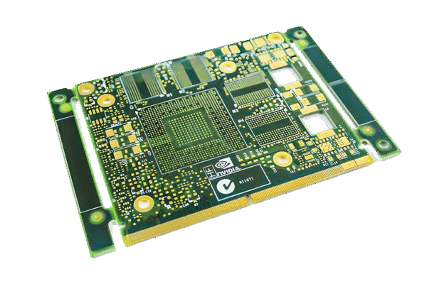
Critical PCB Design Challenges for GaN Systems
To unleash Gallium Nitride’s full potential, PCBs must overcome three key hurdles:
| Design Challenge | Impact if Ignored | PCB-Centric Solutions |
| High-Frequency Noise | Signal integrity loss, EMI failure | 4-6 layer HDI with impedance control (±5%), dedicated ground planes, <40µm traces |
| Thermal Stress | Device degradation, lifespan drop | Metal-core PCBs (Aluminum Nitride), thermal vias, <2.2W/mK thermal resistance substrates |
| Power Density | Routing congestion, reliability risks | Any-layer HDI, via-in-pad, embedded passive components |
Material Selection is Critical:
– AlN Ceramic PCBs: Essential for laser drivers (180–260 W/mK thermal conductivity).
– High-Tg Rogers Laminates: Optimal for RF/power fusion circuits (e.g., smartphone PMICs).
– Flex PCBs: Enable curved/foldable device integration.
Reliability Breakthroughs Enabling Mass Adoption
Early GaN devices faced field failure concerns. Recent advances address this:
– JEDEC-Compliant Validation: Leaders like BOE HC Semi now guarantee 1,000+ hour operational reliability for consumer Gallium Nitride chips under JEDEC stress tests.
– Advanced Packaging: STMicroelectronics’ 2SPAK and wire-bond-free designs eliminate thermal fatigue points in high-power adapters.
– Cost Reduction: Companies like GaFuture slashed production costs by 50% in 3 years through 8-inch wafer migration and DPW optimization, making GaN cheaper than silicon equivalents.
SysPCB’s GaN-Optimized PCB Solutions
We empower consumer brands to leverage GaN’s potential through:
1.High-Frequency Expertise
–Impedance-Controlled HDI: 4–12 layer stackups with ≤40µm line/space for 100+ MHz switching.
–EMI-Optimized Layouts: Partitioned analog/digital zones and shielded differential pairs (e.g., USB-PD/MIPI).
2.Thermal Management Mastery
–Embedded Copper Coin + Thermal Vias: Dissipate 15W+ heat without heatsinks in chargers.
–Ceramic Hybrid FR-4: Combines AlN patches with FR-4 for cost-sensitive thermal designs.
3.Miniaturization Technologies
–Any-Layer mSAP: 30/30µm trace/space for Gallium Nitride PMIC fanout.
–Component Embedding: Passives buried within layers to save 60% surface area.
4.Reliability Assurance
–IST & TCT Testing: Validates performance under thermal cycling (-55°C to 150°C).
–AEC-Q200 Compliance: For automotive-adacent consumer devices (e.g., EV travel adapters).
The Future: AI-Driven GaN Architectures & Emerging Opportunities
1.AI-Integrated Power Systems
Next-gen Gallium Nitride controllers (e.g., Navitas’ GaNSense) embed real-time current/temperature monitoring, enabling adaptive power delivery for AI PCs and AR glasses.
2.Sustainable Electronics
GaN’s 30% energy savings could reduce global CO₂ by 2.4Mt/year if deployed in all consumer chargers.
3.Voltage Scaling
900V–1200V GaN platforms (BOE HC Semi, Sanan) will enable single-cable 240W laptop charging and all-in-one kitchen appliances.
Conclusion: Lead the Consumer Power Revolution
Consumer Gallium Nitride isn’t just a component upgrade—it’s the foundation for thinner, greener, and more intelligent electronics. With 78% CAGR growth through 2025, early adopters will dominate markets from fast charging to AI edge devices.
SysPCB delivers the advanced PCBs that make high-performance GaN systems possible:
– Any-layer HDI for ultra-dense Gallium Nitride integrations
–Thermal superhighways for 200W+ designs
–JEDEC-ready reliability for mass production
Ready to design winning Gallium Nitride products?
→ [Contact our GaN PCB specialists for a design review]
→ [Download our “GaN PCB Layout Checklist”]
→ [Explore our 10-layer HDI GaN reference design]