Table of Contents
What is 3D ToF & How Does It Revolutionize Sensing?
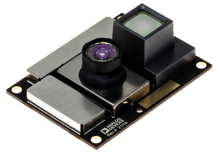
Time-of-Flight (ToF) technology measures the time taken for modulated near-infrared light to reflect off objects, converting phase differences into precise depth maps. Unlike stereoscopic imaging (low accuracy, computationally heavy) or structured light (limited range), ToF offers cm-level accuracy, long-range detection (up to 100 meters), and robust performance in dynamic lighting conditions. This enables real-time 3D mapping for applications from robotics to autonomous driving.
The global 3D industrial vision market is projected to reach ¥3.4 billion (USD 480 million) by 2025, growing at a 22% CAGR. This surge is fueled by demand for smarter automation, AR/VR, and safety-critical systems.
Key Applications Driving Demand for ToF Systems
1.Industrial Automation & Quality Control
–Electronics Manufacturing: Detects PCB warping as fine as 0.01 mm, increasing yield to 99.98%. ToF-guided systems inspect solder joints, component alignment, and micro-defects (e.g., shorts, cracks) with 99.8% accuracy.
–Semiconductor: Measures wafer surface roughness down to 0.1 nm using confocal imaging, surpassing optical microscopes.
–Automotive: Enables 0.05-mm precision in door seam assembly and monitors driver fatigue via eye-tracking (<2 ms latency).
2.Robotics & Logistics
AGVs equipped with ToF cameras achieve 99.5% grab success rates for randomly placed items. In warehouses like JD.com’s Asia No. 1, they process 3,000 parcels/hour—5× faster than manual labor.
3.Consumer Tech & Healthcare
–Smartphones use ToF for AR try-ons, gesture control, and portrait mode.
–Surgical robots like Da Vinci leverage ToF for 0.1-mm precision in real-time organ modeling.
Why Advanced PCBs Are Critical for ToF Performance
ToF systems demand PCBs that resolve four core challenges:
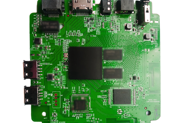
1. Signal Integrity & Speed
High-frequency signals (e.g., MIPI differential lines) require impedance-controlled routing (e.g., 3.5-mil width, 6.5-mil spacing). Solutions like 4-layer HDI stacks dedicate layers to high-speed signals, grounding, and low-speed traces—separated by ≥3× line width to cut EMI.
2.Thermal Management
Laser drivers (e.g., VCSELs) pulse currents up to 28 A with widths as low as 1.2 ns, generating significant heat. Aluminum Nitride (AlN) ceramic PCBs dissipate heat 50× faster than FR-4 (180–260 W/mK vs. 0.3 W/mK), preventing signal distortion.
3.Miniaturization
Compact ToF modules (e.g., 5 mm × 5 mm evaluation boards) use Any-layer HDI and embedded components (e.g., drivers in substrate cavities) to shorten signal paths, reduce inductance, and boost density.
4.Reliability in Harsh Environments
Automotive/industrial ToF PCBs need AEC-Q101 compliance and ESD protection. Full-copper grounding layers (IPC Class 3) shield against interference in high-vibration settings.
PCB Material Comparison for ToF Applications
| Material | Thermal Conductivity | CTE Match w/Si | Min. L/S | Best For |
| AlN Ceramic | 180–260 W/(mK) | Excellent | 20 μm | High-power laser drivers |
| FR-4 | 0.3 W/(mK) | Poor | 75 μm | Cost-sensitive designs |
| High-Tg Rogers | 0.6–1.2 W/(mK) | Good | 40 μm | RF/high-frequency circuits |
| Flexible PI | 0.2 W/(mK) | Moderate | 50 μm | Wearables/compact modules |
SysPCB’s Expertise in ToF-Optimized PCBs
We enable next-gen ToF systems through:
1. High-Density Interconnect (HDI) Mastery
– Any-layer microvias (≤40-μm traces) and via-in-pad for ultra-compact laser/CMOS layouts.
– Sequential lamination for layer-by-layer via drilling, critical for 8+ layer ToF controllers.
2.Material Science Leadership
Partnerships with AlN ceramic suppliers deliver >99% thermal reliability in automotive-grade ToF drivers.
3.Signal/Power Integrity Optimization
Our DFM services model EMI risks for 100+ MHz signals, recommending stackups like:
–Layer 1: Short low-speed traces + components
–Layer 2: High-speed routing (MIPI, USB, SPI)
–Layer 3: Solid ground plane
–Layer 4: Power + low-speed
4.Rigorous Testing & Compliance
Automated optical inspection (AOI), IST reliability testing, and AEC-Q101 certification for automotive ToF modules.
The Future: ToF and the AI-IoT Convergence
Emerging trends demand more advanced PCBs:
– Edge AI ToF sensors (e.g., Melexis’ 640 × 480 VGA resolution) require 10+ layer boards with >10 Gbps data lanes.
– Low-power wearable ToF needs ultra-thin flexible PCBs with stretchable interconnects.
– Automotive cocooning systems (e.g., driver drowsiness detection) rely on robust ceramic PCBs for 150-meter object identification.
Partner with Us for Your ToF Breakthroughs
SysPCB combines deep expertise in high-frequency, thermal-efficient PCB design with semiconductor-grade manufacturing. Our solutions power ToF cameras achieving:
– 99.8% defect detection accuracy in PCB production lines
– 0.1-mm surgical precision in medical robots
– <1.2 ns laser pulses for LiDAR
Ready to innovate with PCBs for 3D ToF?
→ [Contact us for a ToF design consultation]
→ [Explore our HDI PCB capabilities]
→ [Download our ToF design guidelines]