The global AR/AI glasses market is accelerating toward an $18.2B valuation by 2029, driven by breakthroughs in generative AI, compact optics, and immersive interfaces. At the core of this transformation lie specialized PCBs that solve unprecedented engineering challenges: enabling real-time AI processing in sub-10mm spaces, supporting 200Gbps data streams, and surviving 100,000+ flex cycles. For PCB manufacturers, this convergence of AI and augmented reality represents a $2B+ near-term opportunity in high-density interconnects, hybrid materials, and photonic integration.
Table of Contents
I. Core Technical Challenges Driving PCB Innovation
1.Extreme Miniaturization
AI glasses demand PCB footprints under 300mm²—smaller than a credit card—while integrating GPU-level processing. This requires:
–20×20μm trace/spacing via mSAP (modified Semi-Additive Process), supporting 50,000+ interconnects/cm²
–Any-layer HDI with stacked microvias (≤60μm diameter) to route beneath chips like Qualcomm’s AR1 Gen 2
–Embedded passives replacing discrete components, saving 40% board area in Rokid’s latest glasses

2.High-Speed Data Transmission
Real-time object recognition and 8K overlays require 200Gbps+ bandwidth with ultra-low latency:
–Low-Dk/Df materials: Megtron 6 (Df<0.001) reduces signal loss to 0.2dB/cm at 60GHz vs. 1.5dB/cm for FR-4
–Impedance control ±3%: Critical for PCIe 6.0 interfaces in Meta’s Celeste glasses
–Shielded trenches: Copper fences between differential pairs suppress crosstalk by 25dB
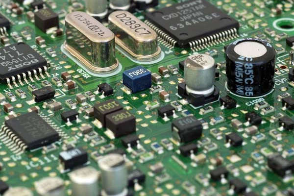
3.Mechanical & Thermal Resilience
PCBs must endure constant flexing while dissipating heat from 10W+ AI chips:
–Polyimide-based flex circuits with 0.05mm thickness sustain >100,000 bends in hinge joints
–Copper-filled microvias and 25μm graphene films reduce hotspot temps by 15°C in Vision Pro equivalents
II. Cutting-Edge PCB Technologies in Current AR/AI Glasses
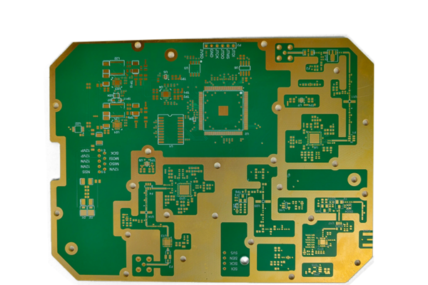
A. High-Density Interconnect (HDI) Dominance
•Meta Celeste (2025): 10-layer any-layer HDI with 30μm laser vias enables 58 PPI display drivers
•Alibaba WOW Glasses: 0.3mm rigid-flex joints allow 15° frame curvature while hosting dual MicroLED projectors
•Medical AR Headsets: 18-layer HDI + embedded NiChrome heaters maintain signal integrity in -40°C surgical environments
B. Material Breakthroughs
| Material | Application | Benefit | Example Use Case |
| LCP Substrates | Antenna arrays | Dk=2.9±0.04 @110GHz; enables 28/140GHz dual-band beamforming | Rokid’s 4-waveguide system |
| Nanoceramics | RF modules | Df<0.001 @300GHz; 40% lower loss than PTFE | Low-orbit satellite-linked glasses |
| Glass Cores | Optical waveguides | CTE=5.5ppm/°C; matches Si photonics chips | Apple’s rumored 2026 waveguide |
C. Photonic-Electronic Fusion
Leading-edge designs integrate optical layers directly into PCBs:
– Quartz-embedded waveguides: 0.3mm deep micro-slots carry light signals at 200Gbps with 0.5dB loss (vs. 5dB for copper)
– Hybrid PCBs: Combine 56Gbps electrical traces + optical lanes in Meta’s Project Orion, slashing power by 60%
III. Supply Chain Shifts & Manufacturing Imperatives
1.Capacity Constraints:
AI glasses PCBs command 5–7× higher ASP than smartphones but require:
–LDI laser drilling: ±2μm positional accuracy for 20μm microvias
–Cationic resin plugging: Prevents copper peeling in via-in-pad structures
Leading manufacturers like Jingwang Electron report 18-month backlogs for 8+ layer HDI orders
2.Cost vs. Performance Tradeoffs:
–Localized material: Chinese BaTiO₃ nanoceramics cost 50% less than Rogers RO3000 series
–Hybrid stackups: Mix FR-4 power layers with Megtron signal layers (30% cost reduction)
3.Geopolitical Diversification:
Thailand/Vietnam now host 35% of global HDI capacity as firms like Shennan Circuits bypass trade barriers
IV. Future Frontiers: 2026–2030 Roadmap
1.Chiplet-Enabled Architectures:
CoWoP (Chip-on-Wafer-on-PCB) will eliminate ABF substrates, placing AI chiplets directly on mSAP PCBs with 25μm lines
2.Self-Healing Circuits:
Micro-encapsulated GaIn alloys automatically repair cracked traces after 10G impact drops
3.Dynamic Impedance Tuning:
AI-driven sensors adjust trace parameters in real-time for -40°C to 85°C environments
4.Sustainable Materials:
Halogen-free resins and recycled copper foils to meet EU carbon tariffs (e.g., 18% lower CO₂/kg by 2027)
V. Strategic Recommendations for PCB Manufacturers
1.Prioritize HDI/mSAP Capabilities: Target ≤25μm lines for CoWoP-ready production lines
2.Forge Optical Partnerships: Collaborate with Luxshare (Apple) or Lumus (Meta) on quartz waveguide integration
3.Adopt AI-Driven Manufacturing:
–Generative design slashes 16-layer layout time from weeks to hours
–AOI with deep learning cuts defect escape by 90%
The winners will be those treating PCBs not as passive carriers, but as active performance enablers for spatial computing.
Conclusion: The Invisible Engine of the AR Revolution
AR/AI glasses represent the most demanding PCB application in consumer electronics history—requering nanometer-scale precision, terahertz bandwidth, and wearable durability. As glass architectures evolve toward photonic integration and heterogeneous chiplets, PCB manufacturers must lead in three domains: material science (low-loss nanoceramics), process innovation (mSAP/POFV), and thermal resilience (embedded cooling).
With 30% of top-tier VR/AR vendors already sourcing advanced PCBs from Chinese suppliers, and glass-core substrates projected to grow at 5.3% CAGR through 2031, the opportunity is both immense and urgent.
Partner with SysPCB for AR-Grade PCBs—leveraging 20μm mSAP technology, 98.2% production yield, and thermal management solutions proven in 10M+ wearable devices. Contact us to co-design your next-gen optical platform.