The prevalence of black PCBs in smartphones isn’t about electrical performance—it’s a strategic choice rooted in aesthetics, advanced manufacturing, and brand positioning.In the tightly packed interior of a modern smartphone, the color of the PCB serves purposes far beyond mere appearance. While green PCBs dominate the broader electronics landscape, smartphone manufacturers, particularly in mid-range and flagship models, consistently opt for black. This article explores the technical, aesthetic, and practical reasons behind this industry preference.
Table of Contents
1.The Basics: What Determines PCB Color?
First, it’s essential to understand that a PCB’s color comes from thesolder mask ink—a protective layer applied over the bare substrate, which is typically semi-transparent or light yellow. This layer insulates copper traces, prevents solder shorts, and safeguards the board from environmental damage. Whether green, blue, or black, the solder mask’s primary function remains the same, provided the ink meets quality standards .
2.5 Key Reasons Smartphones Favor Black PCBs
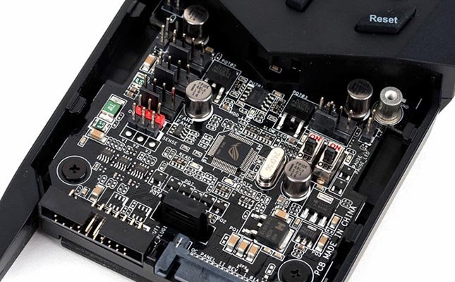
1. Aesthetic Appeal and Perceived Quality
Black is universally associated with sophistication, precision, and high quality. In a smartphone’s compact interior, components like chips, resistors, and capacitors vary in color (silver, green, gold, etc.). A black PCB acts as aunified backgroundthat minimizes visual clutter, allowing the board to appear neat, integrated, and technologically advanced. This is critical for brands aiming to convey a premium feel when consumers or reviewers examine the device’s interior .
2. Demonstration of Manufacturing Expertise
Producing black PCBs is technically challenging. The dark, opaque pigment requireshigh-precision exposure and alignmentduring fabrication. Even minor deviations in dust control or exposure settings can lead to noticeable defects, lowering yield rates. Thus, using black PCBs signals a manufacturer’s advanced工艺 capabilities and strict quality control—a silent boast of their production prowess .
3. Functional Benefits: Light Absorption and Sensors
Black PCBs helpreduce internal light reflection. Smartphones house numerous sensors (e.g., proximity sensors, cameras), and stray light can interfere with their accuracy. The dark surface absorbs stray light, improving sensor reliability. Additionally, while the effect is minimal, black theoretically enhances heat radiation, offering a minor advantage in thermal management alongside dedicated cooling solutions like copper foil and heat spreaders .
4. A Deterrent to Reverse Engineering
Though not foolproof, black PCBs candeter casual copying. Traces are harder to distinguish with the naked eye or basic scanners, raising the barrier for competitors attempting to photograph and replicate designs. However, specialized reverse-engineering teams can still overcome this with advanced imaging techniques .
5. Brand Differentiation and Market Positioning
Black PCBs are predominantly used inhigh-end devices(e.g., Apple, Samsung, Huawei flagships), while green PCBs are more common in budget models. This divergence reinforces brand perception: black implies luxury and innovation, whereas green emphasizes cost-effectiveness. The higher cost of black PCBs—driven by lower yields and tougher工艺—makes them a deliberate investment for premium branding .
3.Why Aren’t All PCBs Black? The Trade-Offs
Despite their advantages, black PCBs have limitations:
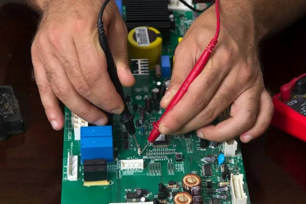
•Debugging Difficulty:The dark background makes it harder to inspect traces, identify test points, or spot defects during R&D and repair. Lighter colors like green offer better contrast for silkscreen labels and circuit tracking .
•Higher Cost:Black PCBs’ lower yield and demanding工艺 increase production costs. Green solder mask ink, in contrast, is inexpensive and widely available, making it ideal for cost-sensitive applications .
•Not Inherently Superior Electrically:Color does not affect electrical performance. Signal integrity depends on materials, layer stack-up, and layout design .
The table below summarizes how black PCBs compare to green ones in smartphone applications:
| Feature | Black PCB | Green PCB |
| Primary Use | High-end smartphones, flagship electronics | Consumer electronics, low-to-mid-range devices |
| Cost | Higher (due to complex工艺 and lower yield) | Lower (mature process, high availability) |
| Aesthetics | Premium, uniform, minimizes visual clutter | Standard, practical, but can appear cluttered |
| Manufacturing Difficulty | High (precision required in exposure/alignment) | Low (成熟工艺, forgiving) |
| Repair & Debugging | Challenging (low contrast for visual inspection) | Easier (high contrast for traces and labels) |
| Sensor Performance | Reduces internal light interference | No significant benefit |
Conclusion: Black PCBs as a Mark of Excellence
The smartphone industry’s preference for black PCBs is a calculated decision aligned with high-end branding. It balances aesthetics, technical sophistication, and functional subtlety, reflecting a manufacturer’s commitment to quality. While green PCBs remain the pragmatic choice for most electronics, black PCBs symbolize a product’s transition from a mere prototype to a refined commercial device .
For PCB manufacturers, offering robust black solder mask solutions—while educating clients on requirements—can be a valuable competitive edge in the mobile electronics market.