Table of Contents
Introduction to UHDI Technology
Ultra High-Density Interconnect (UHDI) technology represents the cutting edge of printed circuit board manufacturing, pushing the boundaries of miniaturization and performance beyond traditional HDI capabilities. As electronic components continue to shrink in size while increasing in complexity, Ultra HDI has emerged as a critical enabling technology for next-generation electronic devices across industries from aerospace to medical technology.
Ultra HDI technology is characterized by significantly reduced feature sizes compared to conventional HDI, typically defined by conductor widths and spacing below 50 μm, dielectric thickness under 50 μm, and microvia diameters smaller than 75 μm – specifications that exceed the current IPC-2226 Class C standards . While formal industry standards are still evolving, with IPC working groups actively developing comprehensive specifications, leading PCB manufacturers are already investing in the specialized equipment and processes necessary to produce these advanced circuits .
This comprehensive guide explores the technical specifications, manufacturing processes, design considerations, and applications of UHDI technology, providing valuable insights for electronics engineers and designers considering this advanced approach for their next-generation products.
1.Technical Specifications and Defining Characteristics
UHDI vs. Traditional HDI: Key Differences
UHDI technology represents a significant advancement over traditional HDI capabilities, with several critical distinguishing characteristics:
•Fine Line Geometry: Ultra HDI circuits typically feature conductor widths and spacing of 20-25 μm, substantially smaller than the 50 μm threshold that defines traditional HDI . This enables dramatically higher circuit density in the same board area.
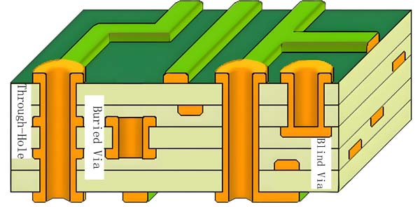
•Advanced Microvia Technology: UHDI implements microvias with diameters smaller than 75 μm, with advanced implementations achieving even smaller dimensions . These microvias can be stacked four layers or more in what’s known as any-layer via structures .
•Ultra-Thin Dielectrics: Ultra HDI employs dielectric layers thinner than 50 μm, enabling improved impedance control and better high-frequency performance . These thin dielectrics also contribute to overall package miniaturization.
•Enhanced Material Properties: UHDI substrates require materials with superior dimensional stability, low loss characteristics, and improved thermal performance to support the fine features and ensure reliability .
Table: Comparison of Traditional HDI vs. UHDI Technical Specifications
| Parameter | Traditional HDI | UHDI |
| Conductor Width/Spacing | ≥50 μm | <50 μm (typically 20-25 μm) |
| Dielectric Thickness | ≥50 μm | <50 μm |
| Microvia Diameter | ≥75 μm | <75 μm |
| Standards Compliance | IPC-2226 Class A-C | Exceeds current IPC standards |
| Typical Applications | Consumer electronics, mobile devices | Aerospace, medical, advanced packaging |
2.UHDI Manufacturing Processes and Technologies
Advanced Fabrication Techniques
Manufacturing UHDI circuits requires specialized approaches beyond conventional PCB fabrication methods:
Modified Semi-Additive Process (mSAP)
The modified Semi-Additive Process (mSAP) has emerged as a critical enabling technology for Ultra HDI manufacturing. Unlike traditional subtractive methods that etch away copper from thick foil, mSAP starts with thin copper deposition followed by selective buildup . This approach offers significant advantages for fine feature creation, including:
– Enhanced line width control and uniformity
– Reduced undercut during etching
– Improved yield for very fine traces
– Better environmental profile through reduced copper usage
Laser Direct Imaging (LDI)
Laser Direct Imaging (LDI) technology is essential for UHDI manufacturing, providing the precision needed to transfer circuit patterns to substrates with the required accuracy . LDI systems eliminate the dimensional stability challenges associated with traditional phototools, enabling finer features and improved registration accuracy.
Advanced Laser Drilling
Creating microvias for Ultra HDI requires sophisticated laser drilling systems capable of producing extremely small, high-quality holes. Some manufacturers are investing in dedicated laser drilling equipment to achieve the necessary via diameters and quality for Ultra HDI applications .
Critical Manufacturing Environment Requirements
UHDI manufacturing demands controlled environments that far exceed standard PCB fabrication facilities:
– Extreme cleanliness to prevent contamination and defects
– Strict temperature and humidity control to maintain dimensional stability
– Advanced air filtration systems to eliminate particulate matter
Manufacturing Challenges and Solutions
UHDI presents significant manufacturing challenges that require specialized approaches:
•Material Handling: Ultra-thin materials require careful handling to prevent damage during processing, necessitating specialized equipment and procedures.
•Registration Accuracy: Maintaining layer-to-layer registration with extremely fine features demands advanced alignment systems and processes.
•Copper Plating Uniformity: Achieving consistent copper deposition in high aspect ratio microvias requires optimized plating chemistry and processes.
•Inspection and Testing: Conventional automated optical inspection (AOI) systems may struggle with UHDI features, requiring upgraded equipment with higher resolution capabilities .
3.UHDI Design Considerations and Guidelines
Layout Strategies for Ultra-High Density
Designing for Ultra HDI requires a different approach compared to traditional PCB layout:
High-Density Fanout for Advanced Components
UHDI technology enables efficient fanout of high-pin-count components with very fine pitch, such as:
– Fine-pitch BGAs (0.5 mm and below)
– Chip-scale packages (0.35 mm and 0.3 mm pitch)
– Advanced processors and FPGAs
With UHDI capabilities, designers can route two or even four traces between BGA pads, significantly reducing the layer count required for component escape . This trace routing density directly translates to reduced layer counts and potentially lower overall costs despite the more advanced manufacturing process.
Impedance Control and Signal Integrity
The ultra-fine features and thin dielectrics in UHDI designs present both challenges and opportunities for signal integrity:
– Thinner dielectrics allow closer proximity to reference planes, potentially improving return paths and reducing crosstalk
– Fine trace widths require careful impedance modeling and simulation
– Advanced materials with controlled dielectric properties are essential for predictable high-frequency performance
Thermal Management Considerations
The high circuit density of Ultra HDI designs creates thermal management challenges that must be addressed during the design phase:
– Embedded thermal management solutions may be necessary for high-power designs
– Thermal via patterns must be optimized for the specific microvia technologies used
– Material selection should consider thermal conductivity as well as electrical properties
Design for Manufacturing (DFM)
Successful Ultra HDI implementation requires close collaboration between designers and manufacturers throughout the design process:
•Early Manufacturer Involvement: Engaging with UHDI manufacturers during the initial design phase is critical for success
•Design Rule Optimization: Manufacturers can provide guidance on design rules that balance performance requirements with manufacturability and cost
•Material Selection Guidance: UHDI manufacturers can recommend materials that have been proven to perform well with their specific processes and equipment
4.Applications and Market Opportunities
Growing UHDI Adoption Across Industries
Ultra HDI technology is enabling advancements across multiple electronics sectors:
Aerospace and Defense
The aerospace and defense sector represents a significant early adopter of UHDI technology, driven by requirements for:
– High reliability in demanding environments
– Miniaturization of avionics and weapon systems
– Performance advantages for communications and sensing systems
– Domestic manufacturing requirements in some countries
Medical Electronics
Medical applications are increasingly adopting UHDI technology for:
– Implantable devices requiring extreme miniaturization
– Diagnostic equipment with higher circuit densities
– Biocompatible materials compatible with Ultra HDI processes
Advanced Packaging and Semiconductor Integration
UHDI technology is blurring the lines between PCB manufacturing and semiconductor packaging:
– Chip-level packaging substrates with fine features
– System-in-package (SiP) implementations
– Heterogeneous integration of multiple dice
High-Performance Consumer Devices
While initially limited to very high-volume consumer products, UHDI is now becoming accessible for lower-volume premium consumer devices, including:
– High-end smartphones and wearables
– Augmented and virtual reality systems
– Compact IoT devices with advanced capabilities
Market Outlook and Adoption Trends
The Ultra HDI market is experiencing significant growth driven by multiple factors:
•Increasing Component Density: Semiconductor manufacturers continue to develop components with finer pitches, driving the need for advanced interconnect solutions
•Technology Accessibility: UHDI manufacturing capabilities, once limited to high-volume Asian manufacturers, are becoming more accessible globally for lower-volume production
•Standardization Efforts: Ongoing work by IPC and other standards organizations is helping to stabilize UHDI technologies and processes

5.Implementation Strategy for PCB Manufacturers
Building UHDI Capabilities
For PCB manufacturers considering UHDI technology adoption, a strategic approach is essential:
Technology Investment
Developing Ultra HDI capabilities requires significant investment in specialized equipment:
– Advanced laser drilling systems for microvia formation
– Laser Direct Imaging (LDI) equipment for fine feature patterning
– Modified Semi-Additive Process (mSAP) lines
– Enhanced inspection systems with higher resolution capabilities
Process Development
Beyond equipment acquisition, successful UHDI implementation requires comprehensive process development:
– Material evaluation and qualification for UHDI applications
– Process parameter optimization for each manufacturing step
– Cleanroom protocols and environmental controls
– Staff training on UHDI-specific requirements and procedures
Business Considerations
The business case for Ultra HDI investment should consider several factors:
– Market positioning as a technology leader
– Return on investment timeline based on target markets
– Pricing strategy for specialized UHDI services
– Partnership opportunities with material and equipment suppliers
6.Future Trends and Development Directions
Technology Evolution
UHDI technology continues to evolve, with several emerging trends shaping its future:
Advanced Materials Development
Material innovations are critical for pushing UHDI capabilities further:
– Ultra-low loss dielectrics for high-frequency applications
– Dimensionally stable substrates for improved registration
– Advanced copper foils with smoother surfaces for finer features
Process Enhancements
Ongoing process improvements aim to enhance Ultra HDI capabilities and accessibility:
– More cost-effective implementation of mSAP and related technologies
– Improved yields through better process control and defect reduction
– Higher productivity equipment to reduce manufacturing costs
Integration with Emerging Technologies
UHDI is converging with other advanced electronic technologies:
– Embedded components within the PCB structure
– Advanced thermal management integration
– Photonic interconnects for mixed signal-photonic applications
Standards Development
The UHDI landscape continues to mature through standardization efforts:
– IPC working groups are actively developing comprehensive UHDI standards
– International standards are evolving to create a consistent framework for UHDI technology
– Quality and reliability standards are being established to ensure consistent performance
Conclusion: Embracing the UHDI Revolution
Ultra High-Density Interconnect technology represents a significant advancement in PCB manufacturing, enabling new possibilities in electronic product design across industries. While implementing UHDI requires substantial investment in specialized equipment, processes, and expertise, the technology offers compelling advantages for applications demanding the highest circuit densities and performance.
For PCB manufacturers, developing Ultra HDI capabilities represents an opportunity to position themselves at the forefront of technology and serve growing markets in aerospace, medical, advanced packaging, and high-performance consumer electronics. Success in UHDI requires close collaboration between designers and manufacturers, careful attention to process details, and a long-term perspective on technology investment.
As electronic devices continue to become smaller, smarter, and more connected, Ultra HDI technology will play an increasingly important role in enabling these advancements. PCB manufacturers who master UHDI processes will be well-positioned to lead the industry into the next generation of electronic innovation.