Table of Contents
Introduction
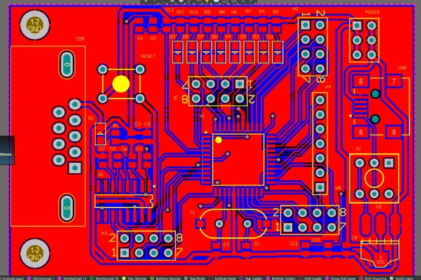
High-Density Interconnect (HDI) Printed Circuit Boards represent a significant advancement in PCB technology, enabling higher circuit density, improved signal integrity, and more compact electronic devices. However, the manufacturing process involves complex procedures that introduce specific challenges and potential defects. Understanding these common issues and implementing appropriate preventive measures is crucial for maintaining high quality standards and production yield. This comprehensive guide examines the most frequent defects encountered in HDI PCB manufacturing and provides practical solutions to address them effectively.
1 Via-Related Defects
1.1 Cracked Core at Via Bottom
The structure with “outer copper layer + laser via copper pillar + copper layer + substrate” is particularly susceptible to cracks at the via bottom core due to heat transfer and stress mechanisms.
Preventive Measures:
– Optimize thermal management during lamination and soldering processes
– Implement controlled thermal stress relief procedures
– Consider alternative via structures for critical applications

1.2 Copper Plating Voids in Blind Vias
Blind via copper plating typically exhibits three common defects: voids, dents, and gaps, with leakage being the most prevalent failure type. These issues often stem from drilling, contamination, or electroplating problems.
Preventive Measures:
– Implement rigorous contamination control throughout the process
– Optimize electroplating parameters specifically for blind vias
– Utilize Horizontal Plating Lines or Vertical Continuous Plating (VCP) lines with high-pressure jet spraying to improve plating quality in microvias
1.3 Resin Debris and Voids
Resin debris accumulation in blind vias can cause copper deficiencies, creating reliability issues in the final product.
Preventive Measures:
– Enhance cleaning procedures after drilling operations
– Implement regular maintenance of drilling equipment
– Establish stringent debris monitoring systems
2 Lamination and Material Defects
2.1 Delamination and Blistering
Delamination primarily occurs in areas with dense buried vias or beneath large copper planes on outer layers. This defect results from volatile substances (including organic compounds and water) expanding rapidly when heated during assembly, with the outer copper layer preventing their escape, thus generating significant internal steam pressure.
Preventive Measures:
– Implement pre-bake procedures to remove moisture before assembly
– Optimize lamination parameters for specific material combinations
– Use materials with lower coefficient of thermal expansion
– Design more balanced copper distribution to minimize stress concentration
2.2 Dimensional Instability
Size deviations can occur throughout the PCB fabrication process due to material expansion and contraction. These variations can cause issues with component placement, soldering, and mechanical fit.
Preventive Measures:
– Maintain consistent environmental controls (temperature and humidity)
– Implement material conditioning before critical processes
– Establish compensation factors based on material behavior
– Utilize Laser Direct Imaging (LDI) equipment for improved pattern transfer accuracy
3 Solder Mask and Surface Finish Defects
3.1 Solder Mask Bubbling and Peeling
Solder mask issues typically result from inadequate process control or incorrect material selection. These defects can lead to corrosion, short circuits, and compromised component soldering.
Preventive Measures:
– Implement proper surface preparation before solder mask application
– Optimize exposure and development parameters
– Select solder mask inks appropriate for specific surface finishes
– Establish comprehensive reliability testing at different production stages
3.2 Galvanic Effect (Galvanic Corrosion)
The galvanic effect occurs in selective gold finishing OSP processes due to the potential difference between gold and copper. This causes connected copper pads to continuously lose electrons and dissolve into divalent copper ions, resulting in reduced pad size that affects component mounting and reliability.
Preventive Measures:
– Implement software-based pad pre-compensation during design
– Establish special rework conditions and limit rework cycles in OSP processes
– Conduct thorough supplier audits to verify capability to address this issue
4 Soldering and Assembly Defects
4.1 BGA Solder Voids
BGA solder voids may cause primary chip function failure and present significant hidden risks as they may not be detected during testing. These voids typically result from residual liquid or impurities in PCB vias that vaporize at high temperatures, or from poor laser via shape on BGA pads.
Preventive Measures:
– Specify electroplated filled vias or semi-filled vias in HDI designs
– Implement proper via treatment before soldering
– Utilize X-ray inspection after component placement
4.2 Poor Solderability
Multiple HDI PCB soldering issues can arise from design limitations, including solder wicking away from components through vias in pads, resulting in poor connections.
Preventive Measures:
– Avoid placing vias directly in solder pads when possible
– Implement via tenting with solder mask when via-in-pad is unavoidable
– Carefully design solder mask openings to prevent excessive solder accumulation

5 Design-Related Issues
5.1 Inadequate Space Management
Higher density HDI designs require careful consideration of layout and spacing factors to ensure manufacturability and maintainability.
Preventive Measures:
– Establish clear DFM guidelines at the beginning of the design process
– Determine appropriate component spacing requirements early
– Consider via diameter, pad diameter, and trace width before finalizing layout
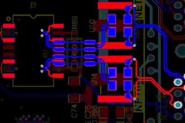
5.2 Improper Via Selection and Implementation
Designers must understand the implications of blind and buried vias as they significantly impact PCB construction methods and can influence signal performance.
Preventive Measures:
– Select via types based on electrical and mechanical requirements
– Consider the impact of via placement on signal integrity
– Consult with manufacturing partners during design phase
Table: Common HDI Manufacturing Defects and Their Impact
| Defect Type | Potential Impact on PCB Function | Detection Methods |
| Via Cracks | Intermittent or complete circuit failure | Cross-section analysis, Thermal cycling |
| Copper Plating Voids | Increased resistance, current carrying capacity reduction | Microsectioning, X-ray inspection |
| Delamination | Reduced thermal performance, mechanical failure | Visual inspection, Acoustic microscopy |
| Solder Mask Defects | Corrosion, short circuits, poor solder joints | Visual inspection, Adhesion testing |
| BGA Solder Voids | Intermittent connections, reduced thermal transfer | X-ray inspection, Functional testing |
6 Critical Process Control Measures
6.1 Advanced Equipment Requirements
Manufacturing HDI circuit boards requires more advanced equipment than conventional multilayer PCBs to achieve the finer feature sizes.
Essential Equipment:
– Advanced laser drilling equipment capable of producing blind holes with diameters of 100μm or less
– High-precision pattern transfer processes utilizing Laser Direct Imaging (LDI) equipment
– Clean rooms with strict temperature and humidity controls, meeting Federal Standard 209E Class 10000 requirements
6.2 Comprehensive Design Review Process
Implementing thorough design reviews is particularly critical for HDI projects due to their complexity and density.
Preventive Measures:
– Establish multidisciplinary review teams including designers, technicians, and manufacturing experts
– Implement formal design review checkpoints throughout the development process
– Utilize design validation tools specifically for HDI requirements
7 Supplier Selection and Quality Assurance
7.1 Manufacturing Process Capability Assessment
When evaluating PCB suppliers for HDI production, it’s essential to conduct comprehensive assessments beyond basic equipment checks.
Key Assessment Factors:
– Examine chemical processes and methodology
– Evaluate graphic transfer equipment and processes
– Review actual experience and data performance in HDI manufacturing
– Verify comprehensive process control systems
7.2 Design for Manufacturing (DFM) Collaboration
PCB suppliers should engage early in the design process to help customers find appropriate solutions that balance performance, complexity, and cost.
Collaborative Approaches:
– Evaluate component selection for economic feasibility and manufacturability
– Assess space requirements versus complexity trade-offs
– Recommend design parameters suitable for volume production
– Provide HDI-specific design guidelines and checklists
Conclusion
Successfully manufacturing HDI PCBs requires addressing numerous potential defects through comprehensive design strategies, precise process controls, and appropriate equipment capabilities. By understanding the common failure mechanisms and implementing the preventive measures outlined in this guide, manufacturers can significantly improve yields and product reliability while reducing costs associated with rework and scrap.
The complex nature of HDI technology demands close collaboration between designers and manufacturers throughout the development process. This partnership, combined with stringent process controls and continuous improvement initiatives, enables the production of high-quality HDI boards that meet the ever-increasing demands of modern electronic devices.
As HDI technology continues to evolve with trends toward higher layer counts, more connections, and finer line widths and spacing, manufacturers must remain vigilant in identifying and addressing new challenges that emerge with these advancing technologies.