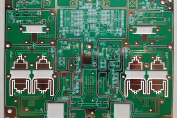
In PCB (printed circuit board) manufacturing, surface treatment processes are crucial for the conductivity, corrosion resistance, and soldering performance of the circuit board. Immersion gold and immersion gold are two common gold layer processing techniques, although they have similar names, there are significant differences in their principles and applications.
Table of Contents
Ⅰ.Immersion Gold (IG) process
Immersion gold is a chemical displacement reaction process that uses copper on the surface of a PCB to displace with a gold salt solution, forming a thin layer of gold on the surface of the copper layer (usually with a thickness of 0.05-0.2 μ m).
-Principle: Gold ions (Au ³ ⁺) obtain electrons from the solution, are reduced to metallic gold (Au), and deposited on the copper surface; At the same time, copper atoms (Cu) lose electrons and are oxidized into copper ions (Cu ² ⁺) that enter the solution. The reaction does not require an external current and belongs to a self limiting process (the reaction automatically stops when the copper surface is completely covered by a gold layer).

-Features: The gold layer is thin and uniform, suitable for scenarios with high flatness requirements (such as BGA pads).
Ⅱ.Electroless Gold, commonly referred to as chemical gold deposition, Electroless Nickel Immersion Gold,ENIG)
Sinking gold is not simply depositing a gold layer, but a composite process of depositing a nickel layer first and then immersing gold on the nickel layer, which is called “chemical nickel plating immersion gold”.
-Principle:
1. Chemical nickel plating: Nickel ions (Ni ² ⁺) are reduced to metallic nickel (Ni) by a reducing agent such as sodium hypophosphite, and deposited on the copper surface to form a nickel layer (usually 2-5 μ m thick) as a barrier layer to prevent copper from diffusing into the gold layer.
2. Gold immersion: A gold layer (thickness 0.05-0.2 μ m) is deposited on the surface of the nickel layer through displacement reaction to protect the nickel layer from oxidation.
-Characteristics: The gold layer adheres to the nickel layer, which enhances mechanical strength and welding reliability. It is currently one of the mainstream surface treatment processes.
Ⅲ. The core difference between immersion gold and immersion gold
| Comparison Dimension | Immersion Gold (Pure Immersion Gold, Non ENIG) | Immersion Gold (ENIG, Chemical Nickel Immersion Gold) |
| Process steps | Single step: direct replacement of gold layer on copper surface | Two steps: chemical nickel plating first, and then immersion of gold on the nickel layer |
| Bottom structure | Gold layer directly covering copper layer | Gold layer covering nickel layer, nickel layer covering copper layer |
| Gold layer thickness | Extremely thin (0.05-0.2 μ m), self limiting unable to increase thickness | Gold layer thickness is similar, but there is a nickel layer at the bottom (2-5 μ m) |
| Function | Only protects the copper layer to prevent oxidation | The nickel layer blocks copper diffusion, the gold layer protects the nickel layer, and enhances weldability |
| Welding reliability | Poor (thin gold layer, easy diffusion of copper to solder joints at high temperatures) | Excellent (nickel layer provides a good welding substrate) |
| Applicable scenarios | Simple PCBs with low reliability requirements, or as temporary protection | High reliability scenarios (such as communication equipment, automotive electronics, BGA) |
Ⅳ.Analysis of the advantages and disadvantages of immersion gold and immersion gold
1. Advantages and disadvantages of immersion gold (pure immersion gold)
-Advantages:
-Simple process and low cost;
-Good uniformity of the gold layer and high surface flatness;
-Suitable for fine wire and dense spacing design (such as fine solder pads).
-Disadvantage:
-Thin gold layer, poor wear resistance, and prone to “copper infiltration” (copper diffusion into the gold layer leading to solder joint failure);
-Low welding reliability, not suitable for high-temperature welding or long-term use;
-Without nickel layer protection, the copper layer is prone to corrosion.
2. Advantages and disadvantages of ENIG
-Advantages:
-The nickel layer serves as a barrier layer, effectively preventing copper diffusion and ensuring high welding reliability;
-The gold layer protects the nickel layer from oxidation, and its corrosion resistance and wear resistance are better than those of pure immersion in gold;
-Suitable for complex environments (such as high temperature, high humidity) and high-frequency signal transmission (gold has excellent conductivity);
-Compatible with multiple soldering processes (reflow soldering, wave soldering, etc.).
-Disadvantage:
-The process is complex and the cost is higher than that of simple immersion in gold;
-Uneven nickel layer thickness may lead to “black disk” defects (nickel layer oxidation, affecting welding);
-High requirements for process control (such as precise control of nickel plating solution composition and temperature).
Ⅴ. Summary
-Simple immersion gold: only suitable for low reliability and low-cost simple PCBs, with limited practical applications.
-ENIG: Due to its reliability and compatibility, it is currently the mainstream process widely used in consumer electronics, automotive electronics, aerospace and other fields.
In actual production, “immersion gold” usually specifically refers to the ENIG process, while pure immersion gold has gradually been phased out due to its limitations, and attention should be paid to avoiding terminology confusion.
Get your exclusive quote immediately: fill out the form or send an email directly.As a professional PCB manufacturer for hobbyist , we will provide you with a quote service within 24 hours. Enjoy free DFM optimization and a 10% discount on SMT patches for your first order!