In modern electronics, data transmission efficiency directly impacts system performance. For PCB designers, choosing between serial and parallel bus architectures involves trade-offs in speed, cost, and signal integrity. Let’s dissect their core differences and why serial buses dominate today’s high-speed designs.
Table of Contents
1、Basic technical differences between serial buses and parallel bus
1. Transmission Mechanism
– Parallel Bus:
Simultaneously transmits multiple data bits (e.g., 8/16/32 bits) across separate wires. Ideal for short-distance communication (e.g., chip-to-chip interfaces), offering high bandwidth but requiring complex wiring. Example: Legacy DDR interfaces use D0–D7 data lines + DQS/DQM control lines, where all signals must arrive synchronously.

– Serial Bus:
Sends data bit-by-bit over a single channel (or differential pairs). Reduces cabling costs and excels in long-distance applications. Modern examples include USB 3.1 (10 Gbps) and PCIe 5.0 (32 GT/s).
2. Physical Design & Signal Challenges
– Parallel:
– Skew Sensitivity: Mismatched trace lengths cause timing skew, forcing PCB designers to use serpentine routing to equalize delays.
– Crosstalk: High-frequency operation exacerbates interference between adjacent wires, limiting max speeds (e.g., IDE capped at 133 MB/s).
– Serial:
– Differential Signaling: Uses paired traces (e.g., USB’s D+/D–) to reject noise, enabling speeds >40 Gbps (Thunderbolt).
– Routing Flexibility: No length-matching needed for single lanes; 10° angled traces minimize signal loss vs. 45°/90° bends.
3. Cost-Power-Space Trade-offs
| Factor | Parallel Bus | Serial Bus |
| Cabling Cost | High (multiple traces) | Low (1-2 traces) |
| Power Use | Higher (simultaneous switching) | Lower (simplex/duplex modes) |
| Board Space | Large (wide buses) | Compact (point-to-point) |
2、Why Serial Buses Are Winning in High-Speed PCB Design
1. Performance Evolution:
Serial protocols like SATA (600 MB/s) replaced PATA/IDE by overcoming parallel’s frequency limitations. As speeds exceed 5 GT/s, serial’s noise immunity outperforms parallel’s multi-path complexity.
2. Material-Driven Innovations:
High-frequency serial designs demand specialized PCB materials:
– Low Dk/Df Laminates: Rogers RO4350B (Df=0.0037) or Megtron6 (Df=0.002) reduce signal attenuation at 10+ GHz.
– Nanoparticle Fillers: Al₂O₃-enhanced resins cut dielectric loss by 40%, critical for 112G PAM4 designs.
3. Real-World Case:
Southeast Mutual Electronics (SME) achieved 18% higher yields in RFPCB production by adopting AI-assisted serial-bus interfaces, slashing misjudgments by 70% during signal integrity checks.
3、PCB Layout Guidelines for Bus Interfaces

– Parallel Routing:
Apply length matching (±5 mil tolerance) and guard traces between clock/data lines to suppress crosstalk.
– Serial Routing:
Prioritize impedance control (e.g., 100Ω for USB). Use ground shields under differential pairs in 28+ GHz mmWave designs.
– Stackup Optimization:
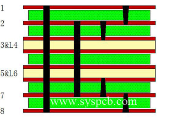
For hybrid designs (e.g., DDR3 + PCIe), separate analog/digital planes. Example 8-layer stack:
`L1: Signal | L2: GND | L3: Parallel Bus | L4: Power | L5: Serial Bus | L6: Split Plane | L7: High-Speed Serial | L8: Signal`
4、Emerging Trends & Your Competitive Edge
1. Next-Gen Standards: PCIe 6.0 (64 GT/s) and USB4 v2 (80 Gbps) will require ultra-low-loss materials like PTFE-ceramic composites (Df<0.0018).
2. AI-Enhanced Validation: Integrate real-time impedance sensors with ML-driven analytics to predict signal faults pre-production.
> Design Tip: Audit legacy parallel interfaces (e.g., LVDS) using DDR-to-SATA bridges to cut costs 25% while upgrading bandwidth.
Conclusion: Future-Proofing Your PCB Strategy
While parallel buses retain niche uses (e.g., memory modules), serial architectures dominate high-speed, noise-sensitive applications. Partner with a specialized PCB manufacturer to leverage:
– Material Selection Tools: Match laminates to bus protocols using Dk/Df databases.
– Signal Integrity Testing: TDR/VNA validation for 56+ Gbps channels.
→ Contact us today for a free design review and download our High-Speed PCB Design Checklist to avoid costly respins.