The Ultimate Guide to Flexible PCB Routing: Design Rules and Manufacturing Best Practices
—
Why Flexible PCB Routing Demands Specialized Approaches
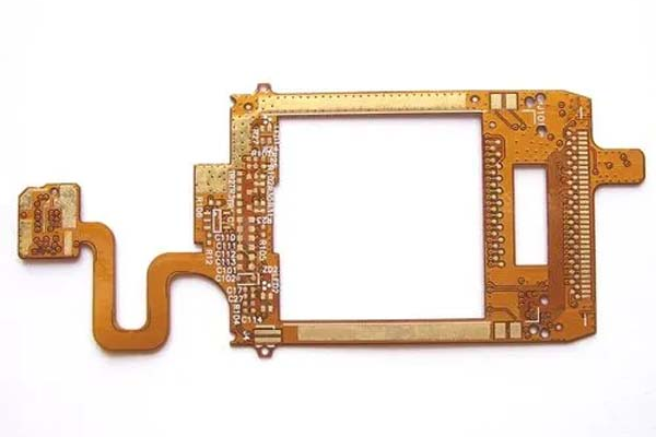
Flexible PCBs enable revolutionary product designs—from wearable medical devices to foldable smartphones—but their dynamic nature introduces unique reliability challenges. Unlike rigid boards, flex circuits endure mechanical stress during bending, requiring specialized routing strategies to prevent trace fractures, delamination, and signal degradation. With the global flex PCB market projected to reach $27 billion by 2028, mastering these techniques is critical for electronics manufacturers targeting cutting-edge applications.
Table of Contents
I. Material Selection: The Foundation of Reliable Flex Routing
1. Base Material Considerations
– Adhesive vs. Adhesiveless Laminates: Adhesiveless polyimide (e.g., DuPont Pyralux AP) offers higher temperature resistance and reduced z-axis expansion, ideal for dynamic flexing. Adhesive-based materials are cost-effective for static bends.
– Copper Types: Rolled annealed (RA) copper withstands repeated bending better than electrodeposited (ED) copper due to its granular structure.
2. Critical Thickness Guidelines
Thicker copper increases rigidity—balance conductivity with flexibility needs.
| Bend Type | Max Copper Thickness | Recommended Layer Count |
| Dynamic (e.g., hinges) | ≤12μm | 1-2 layers |
| Static (e.g., folded once) | ≤35μm | ≤4 layers |
II. Routing Topology: Minimizing Mechanical Stress
1. Bend-Aware Trace Geometry
– Arc Routing: Replace 45°/90° angles with smooth arcs (radius ≥10x trace width) to distribute bending stress evenly. Example: A 0.2mm trace should use ≥2mm arc radii.
– Avoid Width Discontinuities: Use tapered transitions when traces connect to pads (teardrops mandatory) to prevent stress concentration points.
2. Layer Stackup Strategies
– Neutral Axis Alignment: Place copper layers equidistant from the stackup centerline during bends to minimize tension/compression forces.
– Staggered Traces: On multilayer flex, offset adjacent layer traces to avoid overlap at bend points ( A vs. B):
| A (Incorrect): Layer 1: ──────────────── Layer 2: ──────────────── B (Correct): Layer 1: ──────────────── Layer 2: ──────────────── |
Overlapping traces create stiff zones prone to cracking.
3. Controlled Impedance in Flex
– Microstrip vs. Coplanar: Use 1.5x wider traces than rigid PCBs for identical impedance. Tip: Simulate with field solvers like Ansys HFSS.
– Ground Plane Optimization: Replace solid copper pours with cross-hatched patterns (hexagonal preferred) to maintain flexibility while providing EMI shielding.
III. Component Placement and Anchoring
1. High-Reliability Zones

– Bend Prohibition Areas: Maintain ≥5mm clearance from bend lines for SMT components. Place ICs parallel to bend axes to distribute stress.
– Reinforcement Techniques:
– FR-4 Stiffeners: 0.2–1.0mm thick, extending ≥0.5mm beyond component edges (e.g., under BGA/QFP).
– Epoxy Underfill: For large components in moderate-bend applications.
2. Pad/Connection Fortification
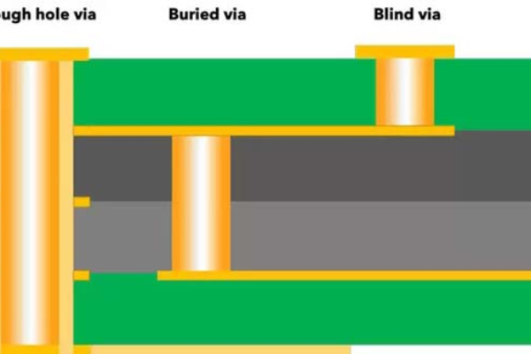
– Plated Through-Holes (PTH): Provide superior anchorage vs. surface pads. Specify 1.5mil extra plating thickness for flex[vitation:1].
– Coverlay Design: Extend openings 0.1–0.15mm beyond pads to prevent adhesive “spill-out” during lamination.
IV. Manufacturing-Driven Design Rules
1. Etching Process Controls
– Acidic Cleaning: Avoid alkaline solutions that swell polyimide. Use pH-balanced cleaners at <50°C.
– Etch Compensation: Add 10–15% trace width tolerance to account for undercutting during flex PCB etching.
2. Lamination and Coverlay
– Vacuum Lamination: Mandatory to eliminate air pockets between layers. Use rigid carrier boards to prevent wrinkling during handling.
– Adhesive Selection: Opt for acrylic-based adhesives (e.g., 3M 467/468) over epoxy for better flex endurance.
V. Advanced Tools for Flex Routing Efficiency
1. Altium ActiveRoute for Complex Layouts
– Guided Routing: Define path constraints with Route Guides to bundle traces through congested areas while maintaining bend rules.
– Differential Pair Support: Automatically routes USB/HDMI pairs with length matching (tolerance ≤0.1mm).
Limitation: Doesn’t support arcs—post-route manual adjustments needed.
2. 3D Co-Design in Autodesk Fusion
– Bend Simulation: Model flex circuits in folded states to identify trace stress hotspots before manufacturing.
– Thermal Analysis: Predict heat buildup in bend zones where cooling is restricted.
VI. Future-Proofing Your Flex Designs
– Embedded Components: Reduce solder joints by integrating passives within flex layers, improving bend reliability.
– Stretchable Circuits: Emerging silver-nanowire inks enable traces that elongate up to 200% without cracking.
– Additive Processing: Laser-direct structuring (LDS) allows 3D molded flex circuits with topology-optimized traces.
> Flex PCBs fail from stress, not electrons. Success hinges on harmonizing electrical needs with mechanical realities—every bend radius decision, trace geometry, and stiffener placement directly impacts field longevity.
Engineer resilience into every curve—transform flex routing from a compromise to a competitive advantage.
Get your exclusive quote immediately: fill out the form or send an email directly.As a professional PCB manufacturer for hobbyist , we will provide you with a quote service within 24 hours. Enjoy free DFM optimization and a 10% discount on SMT patches for your first order!